U.S. Pat. No. 8,188,875
RADIO FIELD INTENSITY MEASUREMENT DEVICE, AND RADIO FIELD INTENSITY DETECTOR AND GAME CONSOLE USING THE SAME
AssigneeSemiconductor Energy Laboratory Co., Ltd.
Issue DateOctober 11, 2011
Illustrative Figure
Abstract
The present invention provides a radio field intensity measurement device having a display portion with improved visibility, in the case of measuring a weak radiowave from a long distance. In the radio field intensity measurement device, a battery is provided as a power source for power supply and the battery is charged by a received radiowave. When a potential of a signal obtained from the received radiowave is higher than an output potential of the battery, the power is stored in the battery. On the other hand, when the potential of the signal obtained from the received radiowave is lower than the output potential of the battery, power produced by the battery is used as power to drive the radio field intensity measurement device. As an element to display the radio field intensity, a thermochromic element or an electrochromic element is used.
Description
DETAILED DESCRIPTION OF THE INVENTION Embodiment Modes Embodiment Modes of the present invention will be explained below with reference to the accompanied drawings. It is easily understood by those skilled in the art that modes and details disclosed herein can be modified in various ways without departing from the spirit and the scope of the present invention. Therefore, the present invention should not be interpreted as being limited to the description of the embodiment modes to be given below. It is to be noted that, in the present invention explained below, there is a case that similar portions or portions having a similar function are denoted by the same reference numerals through the drawings. Embodiment Mode 1 Embodiment Mode 1 will describe a structure of a radio field intensity measurement device of the present invention. FIG. 1is a block diagram of a radio field intensity measurement device of the present invention. The radio field intensity measurement device100includes an antenna110, a rectifier circuit111, a control circuit112, a battery113, an amplifier circuit114and a display element115. Note that the rectifier circuit111, the control circuit112and the amplifier circuit114are collectively referred to as a signal processing circuit120for simple description. FIG. 2is a block diagram in which the antenna110receives a received radiowave302from a radiowave source301. InFIG. 2, the radiowave received by the antenna110is converted into an induction signal and input into the rectifier circuit111. The rectifier circuit111converts the induction signal to a direct signal and outputs the direct signal. In addition, the direct signal output from the rectifier circuit111is input into the battery113through the control circuit112. Meanwhile, the direct signal output from the rectifier circuit111is amplified by the amplifier circuit114and input into the display element115. The display element115changes color in accordance with the direct signal amplified by the amplifier circuit114. The rectifier circuit111, for example as ...
DETAILED DESCRIPTION OF THE INVENTION
Embodiment Modes
Embodiment Modes of the present invention will be explained below with reference to the accompanied drawings. It is easily understood by those skilled in the art that modes and details disclosed herein can be modified in various ways without departing from the spirit and the scope of the present invention. Therefore, the present invention should not be interpreted as being limited to the description of the embodiment modes to be given below. It is to be noted that, in the present invention explained below, there is a case that similar portions or portions having a similar function are denoted by the same reference numerals through the drawings.
Embodiment Mode 1
Embodiment Mode 1 will describe a structure of a radio field intensity measurement device of the present invention.
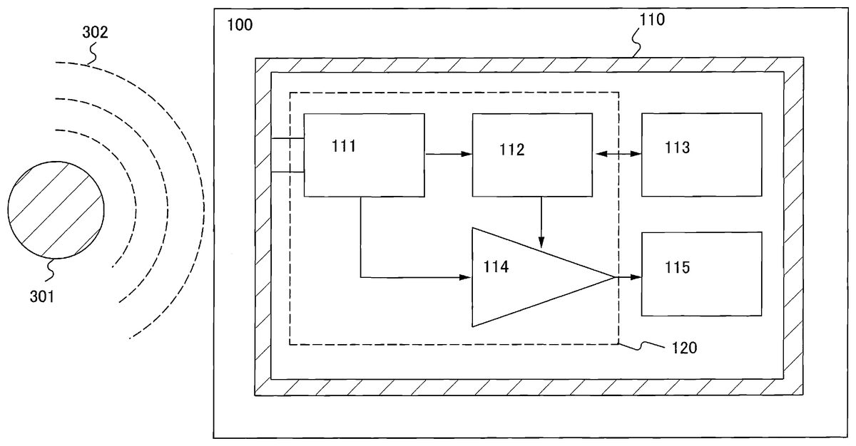
FIG. 1is a block diagram of a radio field intensity measurement device of the present invention. The radio field intensity measurement device100includes an antenna110, a rectifier circuit111, a control circuit112, a battery113, an amplifier circuit114and a display element115. Note that the rectifier circuit111, the control circuit112and the amplifier circuit114are collectively referred to as a signal processing circuit120for simple description.
FIG. 2is a block diagram in which the antenna110receives a received radiowave302from a radiowave source301. InFIG. 2, the radiowave received by the antenna110is converted into an induction signal and input into the rectifier circuit111. The rectifier circuit111converts the induction signal to a direct signal and outputs the direct signal. In addition, the direct signal output from the rectifier circuit111is input into the battery113through the control circuit112. Meanwhile, the direct signal output from the rectifier circuit111is amplified by the amplifier circuit114and input into the display element115. The display element115changes color in accordance with the direct signal amplified by the amplifier circuit114.
The rectifier circuit111, for example as illustrated inFIG. 4, a diode503, a diode504, and a capacitor505, and an induction signal received by the antenna110is half-wave rectified by the diode504and smoothed by the capacitor505. The direct signal which is output from the rectifier circuit111and which is half-wave rectified and smoothed is supplied to the control circuit112.
The control circuit112, for example as illustrated inFIG. 5, includes a diode604, a diode605, a voltage comparison circuit601, a switch602and a switch603.
The voltage comparison circuit601compares an output potential of the battery113with a potential of a direct signal output from the rectifier circuit111. When the potential of the direct signal output from the rectifier circuit111is sufficiently higher than the output potential of the battery113, the voltage comparison circuit601turns the switch602on and the switch603off. Thus, current flows to the battery113from the rectifier circuit111through the diode604and the switch602. On the other, hand, when the potential of the direct signal output from the rectifier circuit111is not sufficiently higher than the output potential of the battery113, the voltage comparison circuit601turns the switch602off and the switch603on. At this time, when the potential of the direct signal output from the rectifier circuit111is higher than the output potential of the battery113, no current flows to the diode605. On the other hand, when the potential of the direct signal output from the rectifier circuit111is lower than the output potential of the battery113, current flows to the amplifier circuit114from the battery113through the switch603and the diode605.
Note that the control circuit is not limited to the example in Embodiment Mode 1, and may employs any mode.
As a switch employed in this specification, a transistor (e.g., a bipolar transistor or a MOS transistor), a diode (e.g., a PN diode, a PIN diode, a Schottky diode, a MIM (Metal Insulator Metal) diode, a MIS (Metal Insulator Semiconductor) diode, or a diode-connected transistor), a thyristor, or the like can be used. Alternatively, a logic circuit combining such elements can be used as a switch.
FIG. 6illustrates an example of the voltage comparison circuit601.
By the voltage comparison circuit601, a voltage output from the battery113is divided by resistors701and702, and a voltage output from the rectifier circuit111is divided by resistors703and704. Then, the voltages divided by the resistors are input to a comparator705. Buffers706and707of inverter topologies are connected in series with an output of the comparator705. Then, an output of the buffer706is input to a control terminal of the switch603, and an output of the buffer707is input to a control terminal of the switch602, so that on/off of the switches602and603inFIG. 6is controlled. Note that when H-level signals are input to the control terminals of the switches602and603, the switches602and603are turned on, whereas when L-level signals are input, the switches602and603are turned off.
By regulating a voltage input to the comparator705by dividing an incoming voltage with the resistors, it becomes possible to control the timings for turning the switch602on and turning the switch603off at a point when the voltage output from the rectifier circuit becomes higher than the voltage output from the battery113by a certain level. Similarly, it becomes possible to control the timings for turning the switch602off and turning the switch603on at a point when the voltage output from the rectifier circuit becomes lower than the voltage output from the battery113by a certain level.
Note that the voltage comparison circuit is not limited to this example in this embodiment mode, and may employ any mode.
With reference to the timing chart ofFIG. 9, operation of the voltage comparison circuit is described. A first waveform1001is a change of a potential after the division by the resistors701and702inFIG. 6. A second waveform1002is a change of a potential after the division by the resistors703and704inFIG. 6. A first signal1010is a control signal which is output from the comparator705and is input to the buffer706inFIG. 6. A second signal1011is a control signal which is output from the buffer706and is input to a control terminal of the switch603inFIG. 6. A third signal1012is a control signal which is output from the buffer707and is input to a control terminal of the switch602inFIG. 6. For simple description, a signal which is input to the rectifier circuit111from the antenna110before rectification is denoted by a waveform before rectification1020(a waveform of an induction signal).
InFIG. 9, when the potential of the first waveform1001is higher than that of the second waveform1002, i.e., when the amplitude of the waveform before rectification which is a signal before rectification is large, the first signal1010is at a high potential level (hereinafter, abbreviated as H), the second signal1011at a low potential level (hereinafter, abbreviated as L), and the third signal1012is H. Accordingly, the switch603to which L of the second signal1011is input is turned off, and the switch602to which H of the third signal1012is input is turned on. Thus, the battery113is charged as illustrated inFIG. 10. The period in which the battery113is charged is regarded as a charge period1030, and during this charge period1030, the amplifier circuit114uses power output from the rectifier circuit111.
InFIG. 9, when the potential of the first waveform1001is lower than that of the second waveform1002, i.e., the amplitude of the waveform before rectification1020which is a signal before rectification, is small, the first signal1010, the second signal1011and the third signal1012are L, H, and L respectively. Accordingly, the switch603to which H of the second signal1011is input is turned on, and the switch602to which L of the third signal1012is input is turned off. Thus, the battery113is discharged as illustrated inFIG. 11. The period in which the battery113is discharged is regarded as a discharge period1031, and during this discharge period1031, the amplifier circuit114uses power output from the battery113.
Therefore, the amplifier circuit114receives power either in the charge period1030or the discharge period1031.
Non-limiting examples of the battery113includes secondary batteries such as a lithium ion battery, a lithium secondary battery, a nickel metal hydride battery, a nickel cadmium battery, and an organic radical battery. Alternatively, a capacitor having large capacity may be used.
Note that the term “charge” indicates that current flows to the battery113, so that power is stored in the battery113. Specifically, in a secondary battery, “charge” means that electric energy input to the battery113is converted to chemical energy to be stored. On the other hand, the term “discharge” indicates that chemical energy in the battery113is converted to electric energy to be output.
A capacitor having large capacity which can be used as the battery113of the present invention is preferably a capacitor having electrodes whose opposed areas are large. In particular, it is preferable to use an electric double layer capacitor which is formed from an electrode material having a large specific surface area such as activated carbon, fullerene, or a carbon nanotube. A capacitor has a simpler structure than a battery. Further, a capacitor can be easily formed to be thin and formed by stacking layers. An electric double layer capacitor has a function of storing power and will not deteriorate so much even after it is charged and discharged a large number of times. Further, the electric double layer capacitor has an excellent property in that it can be charged rapidly.
For the display element115, an element including a material exhibiting a chromism phenomenon, such as a thermochromic material or an electrochromic material, can be used, but not limited to such an element.
Next, with reference to the timing chart ofFIG. 12, operation of the radio field intensity measurement device is described. A first waveform1201is a potential change of a direct signal which is rectified in the rectifier circuit111and is input to the amplifier circuit114inFIG. 2. A second waveform1202is a potential change of a signal which is output from the control circuit112and is input to the amplifier circuit114as power inFIG. 2. Note that the second waveform1202is the same as the second waveform1002inFIG. 9. A third waveform1203is a potential change of voltage, which is obtained by amplifying the first waveform1201input into the amplifier circuit114inFIG. 2with the amplifier circuit114to be input to the display element115. For simple description, a signal which is input to the rectifier circuit111from the antenna110before rectification is denoted by a waveform before rectification1220(a waveform of an induction signal). A period in which the waveform before rectification1220is small is denoted by a weak radiowave period1221, and a period in which the waveform before rectification1220is large is denoted by a strong radiowave period1222, and the minimum operation voltage of the display element115is denoted by reference numeral1223. The minimum operation voltage is a minimum voltage at which the display element115can cause color change which is visible to human eyes.
InFIG. 12, in the weak radiowave period1221, the first waveform1201is amplified as shown by the third waveform1203. In addition, also in the strong radiowave period1222, the first waveform1201is amplified as shown by the third waveform1203. In this case, the ratio of increase from the first waveform1201to the third waveform (V2/V1) is referred to as an amplification ratio. Note that the amplifier circuit114may have such an amplification ratio that the third waveform after amplification exceeds the minimum operation voltage1223.
Therefore, the display element115can operate either in the weak radiowave period1221or the strong radiowave period1222.
Then,FIG. 7Aschematically illustrates of a radio field intensity measurement device of the present invention.
The radio field intensity measurement device illustrated inFIG. 7Aincludes an antenna810, a signal processing circuit811, a battery812and a display element813over a substrate801. The antenna810includes a connection terminal820and a connection terminal821. The connection terminals820and821of the antenna810are both connected to the signal processing circuit811.
As a transistor which can be used for the signal processing circuit811, various types of transistors can be applied without being limited to particular types of transistors. Accordingly, a thin film transistor (TFT) using a non-single crystalline semiconductor film typified by amorphous silicon or polycrystalline silicon, a transistor formed by using a semiconductor substrate or an SOI substrate, a MOS transistor, a junction transistor, a bipolar transistor, a transistor using a compound semiconductor such as ZnO or a-InGaZnO, a transistor using an organic semiconductor or a carbon nanotube, or other transistors can be applied. Note that a non-single crystalline semiconductor film may include hydrogen or halogen.
In addition, various types of substrates can be employed as the substrate801without particular limitations. Accordingly, for example, a single crystalline substrate, an SOI substrate, a glass substrate, a quartz substrate, a plastic substrate, a paper substrate, a cellophane substrate, a stone substrate, or the like can be used. In addition, the signal processing circuit811may be formed over one substrate, and then the signal processing circuit811may be transferred to another substrate.
There are no particular limitations on the shape of the antenna810. For example, as illustrated inFIG. 3A, an antenna403may be provided in the whole area around a signal processing circuit402over a substrate401. As illustrated inFIG. 3B, a thin antenna403may be provided in the area around the signal processing circuit402over the substrate401. As illustrated inFIG. 3C, the antenna may have such a shape that receives a high frequency electromagnetic wave. As illustrated inFIG. 3D, the antenna may have a 180-degree nondirectional shape. As illustrated inFIG. 3E, the antenna may have a stick-like elongated shape. For example, the shape such as a so-called dipole antenna, a loop antenna, a Yagi antenna, a patch antenna, or a minute antenna can be employed.
AlthoughFIGS. 3A to 3Edo not illustrate elements corresponding to the battery and the display element for simple description, the radio field intensity measurement device according to Embodiment Mode 1 includes a battery and a display element.
The antenna810illustrated inFIG. 7Amay be formed over the substrate provided with the signal processing circuit811or a substrate different from the substrate provided with the signal processing circuit811. Various types of substrates can be used as a substrate to be provided with the antenna810, and not-limiting examples of the substrate includes a single crystalline substrate, an SOI substrate, a glass substrate, a quartz substrate, a plastic substrate, a paper substrate, a cellophane substrate, a stone substrate and the like. In the case where the antenna810is formed over the same substrate as the signal processing circuit811, the antenna810may be formed by depositing a conductive film by sputtering, CVD, spin coating, or the like and then patterning the conductive film; or the antenna810may be formed by a droplet discharge method typified by an ink-jet method, a screen printing method, or the like. Also in the case where the antenna810is formed over a substrate which is different from the substrate over which the signal processing circuit811is formed, the antenna810can be formed by any of the aforementioned methods; however, preferably, the antenna810is formed by the screen printing method.
There are no particular limitations on the method of connecting the substrate provided with the signal processing circuit to the antenna. For example, wire bonding or a bump may be adopted to connect the antenna and the substrate provided with the signal processing circuit, or a method where a surface of the substrate provided with a signal processing circuit formed in a chip form is made as an electrode and the electrode is attached to the antenna may be employed. In this method, an anisotropic conductive film (ACF) can be used to connect the antenna and the substrate.
In addition, an appropriate length of the antenna varies depending on a frequency for receiving signals. For example, when the frequency is 2.45 GHz, a half-wave dipole antenna may have a length of a half wavelength (about 60 mm), or a monopole antenna may have a length of a quarter wavelength (about 30 mm).
The antenna may include a means of changing frequency of a received signal. For example, when a loop antenna is used for the antenna, a resonant circuit may be formed from an antenna coil901and a capacitor902included in the antenna110as illustrated inFIG. 8.
Further, inFIG. 7A, the antenna810is formed over the same substrate as the signal processing circuit811, or may be provided as an external antenna. As illustrated inFIG. 7A, when the antenna810is formed over the same substrate801as the signal processing circuit811, the shape of the antenna is preferably a shape of a minute loop antenna, a minute dipole antenna or the like.
As the battery812, secondary batteries can be used, such as a lithium ion battery, a lithium secondary battery, a nickel hydride battery, a nickel cadmium battery, an organic radical battery, a lead-acid battery, an air secondary battery, a nickel zinc battery, a silver zinc battery, and the like. The battery is not limited to these examples, and a high-capacity capacitor may be used. In particular, a lithium ion battery and a lithium secondary battery have high charging and discharging capacity. Therefore, such a lithium ion battery or such a lithium secondary battery can be used as a battery provided for the radio field intensity measurement device of Embodiment Mode 1 in the present invention, and thus miniaturization thereof can be achieved. It is to be noted that an active material or an electrolyte of a lithium ion battery is formed by a sputtering method; therefore, the battery812may be formed over a substrate over which the signal processing circuit811is formed or a substrate over which the antenna810is formed. The battery812is formed over the substrate over which the signal processing circuit811or the antenna810is formed, and thus yield is improved. In a metal lithium battery, a transition metal oxide including lithium ions, a metal oxide, a metal sulfide, an iron compound, a conductive polymer, an organic sulfur compound, or the like is used for an anode active material; lithium (alloy) is used for a cathode active material; and an organic electrolyte solution, a polymer electrolyte, or the like is used for an electrolyte. Therefore, the battery812can have higher charging and discharging capacity.
For the display element813, an element including a material exhibiting chromism phenomena, such as a thermochromic material or an electrochromic material, can be used, but not limited to this element. In particular, as an element including a thermochromic material (also referred to as a thermochromic element), an element including a thermotropic liquid crystal (also referred to as a thermochromic liquid crystal), especially an element including a cholesteric liquid crystal is preferable, and the cholesteric liquid crystal may include cholesteryl oleyl carbonate, cholesteryl nonanoate, or cholesteryl benzoate. In addition, as the element including the electrochromic material (also referred to as an electrochromic element), an element including a metal oxide such as tungsten oxide or a related compound thereof may be used.
The structure of the radio field intensity measurement device according to Embodiment Mode 1 in the present invention is not limited to that ofFIG. 7A. For example, inFIG. 7B, the signal processing circuit811is provided between the antenna810and the battery812; however, the battery812may be provided between the antenna810and the signal processing circuit811or the antenna810may be provided between the battery812and the signal processing circuit811. The area ratio of the antenna810, the battery812and the signal processing circuit811is not limited to the example ofFIGS. 7A and 7B. In other words, in the case where each layer in the cross-section of the radio field intensity measurement device according to this embodiment mode in the present invention is seen, there are no particular limitations on the positional relationship of the antenna810, the battery812and the signal processing circuit811. In addition, the antenna810and the signal processing circuit811may be formed over different substrates, or the antenna810, the signal processing circuit811, and the battery812may be formed over the same substrate. Note that, preferably, the display element813is disposed in the uppermost layer for improving visibility and has a large area.
The radio field intensity measurement device of Embodiment Mode 1 in the present invention has a battery which can store power, and replacing batteries is not needed. Furthermore, even when a received signal is weak, power can be supplied from the battery to the signal processing circuit, and thus the radio field intensity measurement device can operate to measure the intensity of the radiowave. In other words, since the radio field intensity measurement device can measure the intensity of the radiowave having a weak signal, sensitivity improvement and stable measurement of the radio field intensity measurement device can be achieved.
Moreover, when a received signal is strong, the battery can be automatically charged, and thus it is unnecessary that a user bothers charging. Needless to say, if the power stored in the battery becomes small, a user can easily charge the battery by himself/herself.
Embodiment Mode 2
Embodiment Mode 2 will describe a mode in which a display element including a thermochromic material is formed.
FIGS. 13A and 13Bschematically illustrate a display element in the present invention. A display element2500includes a resistance heating element2502, a thermochromic material2503, a transparent substrate2504, a connection terminal2510and a connection terminal2511over a light-shielding substrate2501. One of the connection terminals2510and2511is connected to a power supply terminal. For example, one of the connection terminals2510and2511is connected to the amplifier circuit114in Embodiment Mode 1. Note that the other of the connection terminals2510and2511, which is not connected to the power supply terminal, is connected to a GND terminal.
The structure of the display element in Embodiment Mode 2 is not limited to that inFIGS. 13A and 13B. For example, the thermochromic material2503is arranged above the resistance heating element2502inFIGS. 13A and 13B; alternatively the resistance heating element2502may be arranged over the thermochromic material2503. The shape and area of the resistance heating element2502and the thermochromic material2503are not limited to those ofFIGS. 13A and 13B. For example, a comb-like shape or a convex-concave shape may be employed. Wider areas of the resistance heating element2502and the thermochromic material2503are preferably in contact with each other to enhance thermal conductivity.
In this embodiment mode, “the resistance heating element” indicates general elements which generate heat by electrical power. The amount of generated heat is changed in accordance with the power amount supplied from a connection terminal to the resistance heating element. Various substances can be used as materials of the resistance heating element in this embodiment mode. Thus, there are no particular limitations on the applicable material for the resistance hating element.
The thermochromic material in this embodiment mode indicates general substances which exhibit thermochromism phenomena. The thermochromism phenomenon is phenomena that color of a material is reversibly changed by heat stimulation. Thus, color is changed depending on the amount of heat supplied from the resistance heating element2502. In other words, color is changed in accordance with the amount of power supplied to the display element through the connection terminal. Various substances can be used as a thermochromic material included in the display element of this embodiment mode. Thus, there are no particular limitations on the type of the applicable thermochromic material.
A cholesteric liquid crystal, which is one example of thermochromic material in this embodiment mode, has a feature that a torsional state of the helix is changed depending on temperature. The molecular structure of the cholesteric liquid crystal and the principal of color change depending on the change of the molecular structure of the cholesteric liquid crystal are described with reference toFIGS. 14A,14B andFIGS. 15A,15B.
The cholesteric liquid crystal preferably includes cholesteryl oleyl carbonate in which one side of a carbonate group2100is bound to a cholesteryl group2101and the other side of the carbonate group is bound to an oleyl group2102which is a straight-chain hydrocarbon group as illustrated inFIG. 14A. InFIG. 14A, cholesteryl oleyl carbonate, a compound in which the carbonate group2100and the oleyl group2102are bound to the cholesteryl group2101is shown. Cholesteryl benzoate, a compound in which a benzoate group2103is bonded to the chlesteryl group2101, instead of the carbonate group2100and the oleyl group2102, as illustrated inFIG. 14B, or cholesteryl nanoate, a compound in which a nanoate group2104is bonded to the chlesteryl group2101, instead of the carbonate group2100and the oleyl group2102, as illustrated inFIG. 14Cmay be used. The mixed ratio of liquid crystal molecules including different straight-chain hydrocarbons such as cholesteryl oleyl carbonate, cholesteryl nanonate, and cholesteryl benzoate is changed to change the color of the cholesteric liquid crystal.
The cholesteric liquid crystal has a helical molecular structure and partially reflects incident light. This reflecting property is changed depending on the torsional state of the helix. For example, a cholesteric liquid crystal molecule having a pitch P selectively reflects only a wavelength (λ=n (refractive index of a cholesteric liquid crystal)×P) of wavelengths included in incident light. For example, the liquid crystal molecule2002ofFIG. 15Ahas a torsion corresponding to ¼ pitch in a distance d between a transparent substrate2000and a light-shielding substrate2001, and thus only a wavelength (λ=n×P=n×4d) of wavelengths included in the incident light2003is selectively reflected. In addition, a liquid crystal molecule2002illustrated inFIG. 15Bhas a torsion corresponding to ¾ pitch in the distance d, and thus a wavelength (λ=n×P=n×4/3d) of wavelengths included in the incident light2003is selectively reflected.
Human eyes recognize a difference in a wavelength of light as a difference of a color. Therefore, reflection light2004ofFIG. 15Aand reflection light2004ofFIG. 15Bhave different wavelengths and are recognized as different colors.
The transparent substrate2000illustrated inFIGS. 15A and 15Bmay be transparent to human eyes. Preferably, the substrate transmits all wavelengths. The light-shielding substrate2001illustrated inFIGS. 15A and 15Bmay be a substrate which is black to human eyes. Preferably, the substrate absorbs all wavelengths.
FIG. 16is a cross-sectional view illustrating a thermochromic element which is a display element including a thermochromic material. Wirings2203aand2203bare provided over the light-shielding substrate2201with a base layer2202interposed therebetween. The wiring2203aand the wiring2203bare connected to a resistance heating element2229in a contact portion2206and a contact portion2207provided in an interlayer insulating film2204and an insulating film2205. The resistance heating element2229generates heat by current flowing between the contact opening portion2206and the contact opening portion2207to heat a thermochromic material2211. Note that the wirings2203aand2203bare connected to connection terminals inFIG. 13.
A transparent substrate2214is disposed opposite to the light-shielding substrate2201. A thermochromic material2211is provided between the light-shielding substrate2201and the transparent substrate2214. The distance between the light-shielding substrate2201and the transparent substrate2214is kept by a spacer2210. After a thermochromic material2211is provided between the light-shielding substrate2201and the transparent substrate2214, the light-shielding substrate2201and the transparent substrate2214are fixed by a sealing material2220. It is preferable that the distance between the light-shielding substrate2201and the transparent substrate2214is narrow, since a small amount of the thermochromic material2211is used and the heat amount of the thermochromic material2211to be heated is small, which achieves rapid color change.
In such a display element, by voltage application to the resistance heating element2229, the heat amount supplied to the thermochromic material2211is changed, and thus the state of the thermochromic material2211is changed, so that a color tone reflection light2231is different from that of incident light2230.
Embodiment 1
Embodiment 1 will describe an example of a method for manufacturing the radio field intensity measurement device shown in the above-described embodiment modes with reference to drawings. In this embodiment, a structure in which an antenna, and a signal processing circuit of the radio field intensity measurement device are formed using thin film transistors over the same substrate will be explained. It is to be noted that when an antenna and a signal processing circuit are formed together over the same substrate, reduction in size of the radio field intensity measurement device can be achieved, which is advantageous. In addition, in this embodiment, an example will be explained, in which a thin-film secondary battery is used as the battery in the signal processing circuit. Needless to say, instead of the secondary battery, a capacitor such as an electric double layer capacitor may be used.
First, a peeling layer1303is formed over one surface of a substrate1301with an insulating film1302interposed therebetween, and then an insulating film1304functioning as a base film and a semiconductor film (e.g., a film containing amorphous silicon)1305are stacked thereover (seeFIG. 17A). It is to be noted that the insulating film1302, the peeling layer1303, the insulating film1304, and the semiconductor film1305can be formed consecutively.
The substrate1301is selected from a glass substrate, a quartz substrate, a metal substrate (e.g., a ceramic substrate or a stainless steel substrate), a semiconductor substrate such as a Si substrate, or the like. Alternatively, a plastic substrate made of polyethylene terephthalate (PET), polyethylene naphthalate (PEN), polyether sulfone (PES), acrylic, or the like can be used. In this process, although the peeling layer1303is provided over the entire surface of the substrate1301with the insulating film1302interposed therebetween, the peeling layer1303can also be selectively formed by photolithography after being provided over the entire surface of the substrate1301.
The insulating films1302and1304are formed using insulating materials such as silicon oxide, silicon nitride, silicon oxynitride (SiOxNy, where x>y>0), or silicon nitride oxide (SiNxOy, where x>y>0) by a CVD method, a sputtering method, or the like. For example, when each of the insulating films1302and1304is formed to have a two-layer structure, a silicon nitride oxide film may be formed as a first insulating film and a silicon oxynitride film may be formed as a second insulating film. In addition, a silicon nitride film may be formed as a first insulating film and a silicon oxide film may be formed as a second insulating film. The insulating film1302functions as a blocking layer which prevents an impurity element contained in the substrate1301from getting mixed into the peeling layer1303or elements formed thereover. The insulating film1304functions as a blocking layer which prevents an impurity element contained in the substrate1301or the peeling layer1303from getting mixed into elements formed over the insulating film1304. In this manner, providing the insulating films1302and1304which function as the blocking layers can prevent adverse effects on the elements formed over the peeling layer1303or the insulating film1304, which would otherwise be caused by an alkali metal such as Na or an alkaline earth metal contained in the substrate1301or by the impurity element contained in the peeling layer1303. It is to be noted that when quartz is used for the substrate1301, for example, the insulating films1302and1304may be omitted.
The peeling layer1303may be formed using a metal film, a stacked structure of a metal film and a metal oxide film, or the like. As a metal film, either a single layer or stacked layers is/are formed using an element selected from tungsten (W), molybdenum (Mo), titanium (Ti), tantalum (Ta), niobium (Nb), nickel (Ni), cobalt (Co), zirconium (Zr), zinc (Zn), ruthenium (Ru), rhodium (Rh), palladium (Pd), osmium (Os), and iridium (Ir), or an alloy material or a compound material containing such an element as its main component. In addition, such materials can be formed by a sputtering method, various CVD methods such as a plasma CVD method, or the like. A stacked structure of a metal film and a metal oxide film can be obtained by the steps of forming the above-described metal film, applying plasma treatment thereto under an oxygen atmosphere or an N2O atmosphere or applying heat treatment thereto under an oxygen atmosphere or an N2O atmosphere, and thereby forming oxide or oxynitride of the metal film on the surface of the metal film. For example, when a tungsten film is provided as a metal film by a sputtering method, a CVD method, or the like, a metal oxide film of tungsten oxide can be formed on the surface of the tungsten film by application of plasma treatment to the tungsten film. In that case, the tungsten oxide can be represented by WOxwhere x is in the range of 2 to 3. For example, there are cases where x is 2 (WO2), x is 2.5 (W2O5), x is 2.75 (W4O11), x is 3 (WO3), and the like. When tungsten oxide is formed, there is no particular limitation on the value of x, and thus, which of the above oxides is to be formed may be determined base on the etching rate or the like. In addition, after a metal film (e.g., tungsten) is formed, an insulating film formed of silicon oxide (SiO2) or the like may be formed over the metal film by a sputtering method, and also metal oxide (e.g., tungsten oxide on tungsten) may be formed on the metal film. Moreover, high-density-plasma treatment as described above may be applied as the plasma treatment, for example. Besides, metal nitride or metal oxynitride may also be formed. In that case, plasma treatment or heat treatment may be applied to the metal film under a nitrogen atmosphere or an atmosphere containing nitrogen and oxygen.
The amorphous semiconductor film1305is formed with a thickness of 25 to 200 nm (preferably, 30 to 150 nm) by a sputtering method, an LPCVD method, a plasma CVD method, or the like.
Next, the amorphous semiconductor film1305is crystallized by laser irradiation. Alternatively, the crystallization of the amorphous semiconductor film1305may be performed by a method combining the laser crystallization with a thermal crystallization method using RTA or an annealing furnace or with a thermal crystallization method using a metal element that promotes the crystallization. After that, the crystallized semiconductor film is etched into a desired shape, whereby crystalline semiconductor films1305ato1305fare formed. Then, a gate insulating film1306is formed so as to cover the semiconductor films1305ato1305f(seeFIG. 17B).
The gate insulating film1306is formed using an insulating material such as silicon oxide, silicon nitride, silicon oxynitride (SiOxNy, where x>y>0), or silicon nitride oxide (SiNxOy, where x>y>0) by a CVD method, a sputtering method, or the like. For example, when the gate insulating film1306is formed to have a two-layer structure, it is preferable to form a silicon oxynitride film as a first insulating film and form a silicon nitride oxide film as a second insulating film. Alternatively, it is also preferable to form a silicon oxide film as a first insulating film and form a silicon nitride film as a second insulating film.
An example of a formation process of the crystalline semiconductor films1305ato1305fis briefly explained below. First, an amorphous semiconductor film with a thickness of 50 to 60 nm is formed by a plasma CVD method. Then, a solution containing nickel which is a metal element that promotes crystallization is retained on the amorphous semiconductor film, which is followed by dehydrogenation treatment (500° C. for one hour) and thermal crystallization treatment (550° C. for four hours). Thus, a crystalline semiconductor film is formed. Then, the crystalline semiconductor film is subjected to laser irradiation and then a photolithography process to form the crystalline semiconductor films1305ato1305f. It is to be noted that crystallization of the amorphous semiconductor film may be performed only by laser irradiation, not by thermal crystallization which uses a metal element that promotes crystallization.
As a laser oscillator used for crystallization, either a continuous wave laser (a CW laser) or a pulsed laser can be used. As a laser that can be used here, there are gas lasers such as an Ar laser, a Kr laser, and an excimer laser; a laser whose medium is single-crystalline YAG, YVO4, forsterite (Mg2SiO4), YAlO3, or GdVO4or polycrystalline (ceramic) YAG, Y2O3, YVO4, YAlO3, or GdVO4doped with one or more of Nd, Yb, Cr, Ti, Ho, Er, Tm, and Ta as a dopant; a glass laser; a ruby laser; an alexandrite laser; a Ti:sapphire laser; a copper vapor laser; and a gold vapor laser. When irradiation is performed with the fundamental wave of such a laser beam or the second to fourth harmonics of the fundamental wave, crystals with a large grain size can be obtained. For example, the second harmonic (532 nm) or the third harmonic (355 nm) of an Nd:YVO4laser (the fundamental wave of 1064 nm) can be used. In this case, a laser power density of approximately 0.01 to 100 MW/cm2(preferably, 0.1 to 10 MW/cm2) is needed, and irradiation is performed with a scanning rate of approximately 10 to 2000 cm/sec. It is to be noted that the laser whose medium is single crystal YAG, YVO4, forsterite (Mg2SiO4), YAlO3, or GdVO4or polycrystalline (ceramic) YAG, Y2O3, YVO4, YAlO3, or GdVO4doped with one or more of Nd, Yb, Cr, Ti, Ho, Er, Tm, and Ta as a dopant; an Ar ion laser, or a Ti:sapphire laser can be used as a CW laser, whereas it can also be used as a pulsed laser with a repetition rate of 10 MHz or more by a Q-switch operation, mode locking, or the like. When a laser beam with a repetition rate of 10 MHz or more is used, a semiconductor film is irradiated with the next pulse during the period in which the semiconductor film has been melted by the laser beam and is solidified. Therefore, unlike the case of using a pulsed laser with a low repetition rate, a solid-liquid interface in the semiconductor film can be continuously moved. Thus, crystal grains which have grown continuously in the scanning direction can be obtained.
The gate insulating film1306may be formed by oxidization or nitridation of the surfaces of the semiconductor films1305ato1305fby the above-described high-density plasma treatment. For example, plasma treatment with a mixed gas of a rare gas such as He, Ar, Kr, or Xe, and oxygen, nitrogen oxide (NO2), ammonia, nitrogen, or hydrogen is conducted. When plasma is excited by the introduction of microwaves, plasma with a low electron temperature and high density can be generated. With oxygen radicals (which may include OH radicals) or nitrogen radicals (which may include NH radicals) which are generated by the high-density plasma, the surfaces of the semiconductor films can be oxidized or nitrided.
By such high-density plasma treatment, an insulating film with a thickness of 1 to 20 nm, typically 5 to 10 nm, is formed on the semiconductor films. Since the reaction in this case is a solid-phase reaction, the interface state density between the insulating film and the semiconductor films can be quite low. Since such high-density plasma treatment directly oxidizes (or nitrides) the semiconductor films (crystalline silicon or polycrystalline silicon), desirably, the insulating film can be formed with extremely little unevenness. In addition, since crystal grain boundaries of crystalline silicon are not strongly oxidized, an excellent state is obtained. That is, by the solid-phase oxidation of the surfaces of the semiconductor films by high-density plasma treatment which is described in this embodiment, an insulating film with a uniform thickness and low interface state density can be formed without excessive oxidation reaction at the crystal grain boundaries.
As the gate insulating film, only an insulating film formed by high-density plasma treatment may be used, or a stacked layer may be employed, which is obtained by deposition of an insulating film such as silicon oxide, silicon oxynitride, or silicon nitride on the insulating film, by a CVD method using plasma or thermal reaction. In either case, a transistor which includes such an insulating film formed by high-density plasma treatment in a part or the whole of its gate insulating film can have reduced characteristic variations.
In addition, the semiconductor films1305ato1305f, which are obtained by irradiation of a semiconductor film with a continuous wave laser beam or a laser beam oscillated with a repetition rate of 10 MHz or more and scanning the semiconductor film with the laser beam in one direction to crystallize the semiconductor film, have a characteristic in that their crystals grow in the beam scanning direction. Transistors are each arranged so that its channel length direction (direction in which carriers move when a channel formation region is formed) is aligned with the scanning direction, and the above-described gate insulating film is combined with the semiconductor film, whereby thin film transistors (TFTs) with high electron field effect mobility and reduced variations in characteristics can be obtained.
Next, a first conductive film and a second conductive film are stacked over the gate insulating film1306. Here, the first conductive film is formed to a thickness of 20 to 100 nm by a CVD method, a sputtering method, or the like. The second conductive film is formed to a thickness of 100 to 400 nm. The first conductive film and the second conductive film are formed of an element selected from tantalum (Ta), tungsten (W), titanium (Ti), molybdenum (Mo), aluminum (Al), copper (Cu), chromium (Cr), niobium (Nb), or the like, or an alloy material or a compound material containing such an element as its main component. Alternatively, the first conductive film and the second conductive film are formed of semiconductor materials typified by polycrystalline silicon doped with an impurity element such as phosphorus. As a combination example of the first conductive film and the second conductive film, a tantalum nitride film and a tungsten film; a tungsten nitride film and a tungsten film; a molybdenum nitride film and a molybdenum film; and the like can be given. Tungsten and tantalum nitride have high heat resistance. Therefore, after forming the first conductive film and the second conductive film, thermal treatment for the purpose of heat activation can be applied thereto. In addition, in the case where a two-layer structure is not employed, but a three-layer structure is employed, it is preferable to use a stacked structure of a molybdenum film, an aluminum film, and a molybdenum film.
Next, a resist mask is formed by photolithography, and etching treatment is conducted to form gate electrodes and gate lines. Thus, gate electrodes1307are formed above the semiconductor films1305ato1305f. Here, a stacked structure of a first conductive film1307aand a second conductive film1307bis shown as an example of the gate electrode1307.
Next, the semiconductor films1305ato1305fare doped with an n-type impurity element at low concentration, using the gate electrodes1307as masks by an ion doping method or an ion implantation method. Then, a resist mask is selectively formed by photolithography, and the semiconductor films1305cand1305eare doped with a p-type impurity element at high concentration. As an n-type impurity element, phosphorus (P), arsenic (As), or the like can be used. As a p-type impurity element, boron (B), aluminum (Al), gallium (Ga), or the like can be used. Here, phosphorus (P) is used as an n-type impurity element and is selectively introduced into the semiconductor films1305ato1305fso as to be contained at concentrations of 1×10¹⁵to 1×10¹⁹/cm3. Thus, n-type impurity regions1308are formed. In addition, boron (B) is used as a p-type impurity element, and is selectively introduced into the semiconductor films1305cand1305eso as to be contained at concentrations of 1×10¹⁹to 1×10²⁰/cm3. Thus, p-type impurity regions1309are formed (seeFIG. 17C).
Subsequently, an insulating film is formed so as to cover the gate insulating film1306and the gate electrodes1307. The insulating film is formed to have either a single layer or a stacked layer of a film containing an inorganic material such as silicon, silicon oxide, or silicon nitride, or a film containing an organic material such as an organic resin by a plasma CVD method, a sputtering method, or the like. Next, the insulating film is selectively etched by anisotropic etching mainly in the perpendicular direction, so that insulating films1310(also referred to as sidewalls) which are in contact with the side surfaces of the gate electrodes1307are formed. The insulating films1310are used as masks in doping for forming LDD (Lightly Doped Drain) regions.
Next, the semiconductor films1305a,1305b,1305d, and1305fare doped with an n-type impurity element at high concentration, using resist masks formed by photolithography, the gate electrodes1307and the insulating films1310as masks. Thus, n-type impurity regions1311are formed. Here, phosphorus (P) is used as an n-type impurity element, and is selectively introduced into the semiconductor films1305a,1305b,1305d, and1305fso as to be contained at concentrations of 1×10¹⁹to 1×10²⁰/cm3. Thus, the n-type impurity regions1311with higher concentration of impurity than that of the impurity regions1308are formed.
Through the above steps, n-channel thin film transistors1300a,1300b,1300d, and1300f, and p-channel thin film transistors1300cand1300eare formed (seeFIG. 17D).
In the n-channel thin film transistor1300a, a channel formation region is formed in a region of the semiconductor film1305awhich overlaps with the gate electrode1307; the impurity regions1311serving as source and drain regions are formed in regions of the semiconductor film1305awhich do not overlap with the gate electrode1307and the insulating film1310; and low concentration impurity regions (LDD regions) are formed in regions of the semiconductor film1305awhich overlap with the insulating film1310, between the channel formation region and the impurity regions1311. Similarly, channel formation regions, low concentration impurity regions, and the impurity regions1311are formed in the n-channel thin film transistors1300b,1300d, and1300f.
In the p-channel thin film transistor1300c, a channel formation region is formed in a region of the semiconductor film1305cwhich overlaps with the gate electrode1307, and the impurity regions1309serving as source and drain regions are formed in regions of the semiconductor film1305cwhich do not overlap with the gate electrode1307. Similarly, a channel formation region and the impurity regions1309are formed in the p-channel thin film transistor1300e. Here, although LDD regions are not formed in the p-channel thin film transistors1300cand1300e, LDD regions may be provided in the p-channel thin film transistors or a structure without LDD regions may be applied to the n-channel thin film transistors.
Next, an insulating film with a single layer structure or a stacked layer structure is formed so as to cover the semiconductor films1305ato1305f, the gate electrodes1307, and the like. Then, conductive films1313electrically connected to the impurity regions1309and1311which form the source and drain regions of the thin film transistors1300ato1300fare formed over the insulating film (seeFIG. 18A). The insulating film is formed with a single layer or a stacked layer, using an inorganic material such as silicon oxide or silicon nitride, an organic material such as polyimide, polyamide, benzocyclobutene, acrylic, or epoxy, a siloxane material, or the like by a CVD method, a sputtering method, an SOG method, a droplet discharging method, a screen printing method, or the like. In this embodiment, the insulating film is formed to have a two-layer structure, and a silicon nitride oxide film is formed as a first insulating film1312aand a silicon oxynitride film is fainted as a second insulating film1312b. In addition, the conductive films1313can form the source and drain electrodes of the thin film transistors1300ato1300f.
Before the insulating films1312aand1312bare formed or after one or both of the insulating films1312aand1312bis/are formed, heat treatment is preferably conducted for recovery of the crystallinity of the semiconductor films, activation of the impurity element which has been added into the semiconductor films, or hydrogenation of the semiconductor films. As the heat treatment, thermal annealing, laser annealing, RTA, or the like may be applied.
The conductive films1313are formed with a single layer or a stacked layer of an element selected from aluminum (Al), tungsten (W), titanium (Ti), tantalum (Ta), molybdenum (Mo), nickel (Ni), platinum (Pt), copper (Cu), gold (Au), silver (Ag), manganese (Mn), neodymium (Nd), carbon (C), and silicon (Si), or an alloy material or a compound material containing the element as its main component by a CVD method, a sputtering method or the like. An alloy material containing aluminum as its main component corresponds to, for example, a material which contains aluminum as its main component and also contains nickel, or a material which contains aluminum as its main component, and also contains nickel and one or both of carbon and silicon. The conductive films1313are preferably formed to have a stacked structure of a barrier film, an aluminum-silicon (Al—Si) film, and a barrier film or a stacked structure of a barrier film, an aluminum silicon (Al—Si) film, a titanium nitride film, and a barrier film. Note that the “barrier film” corresponds to a thin film formed of titanium, titanium nitride, molybdenum, or molybdenum nitride. Aluminum and aluminum silicon are suitable materials for forming the conductive films1313because they have low resistance value and are inexpensive. When barrier layers are provided as the top layer and the bottom layer, generation of hillocks of aluminum or aluminum silicon can be prevented. In addition, when a barrier film formed of titanium which is an element having a high reducing property is formed, even when there is a thin natural oxide film formed on the crystalline semiconductor film, the natural oxide film can be chemically reduced, and a favorable contact between the conductive film1313and the crystalline semiconductor film can be obtained.
Next, an insulating film1314is formed so as to cover the conductive films1313, and conductive films1315aand1315belectrically connected to the conductive films1313which form the source electrodes or the drain electrodes of the thin film transistors1300aand1300fare formed over the insulating film1314. In addition, a conductive film1316electrically connected to the conductive film1313which forms the source electrode or drain electrode of the thin film transistor1300bis formed. It is to be noted that the conductive films1315aand1315band the conductive film1316may be formed using the same material at the same time. The conductive films1315aand1315band the conductive film1316can be formed using any of the above-described materials for the conductive film1313.
Next, a conductive film1317functioning as an antenna is formed so as to be electrically connected to the conductive film1316(seeFIG. 18B).
The insulating film1314can be formed with a single layer or a stacked layer of an insulating film containing oxygen and/or nitrogen such as silicon oxide (SiOx), silicon nitride (SiNx), silicon oxynitride (SiOxNywhere x>y>0), or silicon nitride oxide (SiNxOywhere x>y>0); a film containing carbon such as DLC (Diamond-Like Carbon); an organic material such as epoxy, polyimide, polyamide, polyvinyl phenol, benzocyclobutene, or acrylic; or a siloxane material such as a siloxane resin by a CVD method, a sputtering method or the like. It is to be noted that a siloxane material corresponds to a material having a bond of Si—O—Si. Siloxane has a skeleton structure with the bond of silicon (Si) and oxygen (O). As a substituent of siloxane, an organic group containing at least hydrogen (e.g., an alkyl group or aromatic hydrocarbon) is used. In addition, a fluoro group may be used as the substituent. Further, both a fluoro group and an organic group containing at least hydrogen may be used as the substituent.
The conductive film1317can be formed of a conductive material by a CVD method, a sputtering method, a printing method such as screen printing or gravure printing, a droplet discharging method, a dispenser method, a plating method, or the like. The conductive film1317is formed with a single layer or a stacked layer of an element selected from aluminum (Al), titanium (Ti), silver (Ag), copper (Cu), gold (Au), platinum (Pt), nickel (Ni), palladium (Pd), tantalum (Ta), or molybdenum (Mo), or an alloy material or a compound material containing such an element as its main component.
For example, when the conductive film1317functioning as an antenna is formed by a screen printing method, the conductive film can be provided by selective printing of a conductive paste in which conductive particles with a grain diameter of several nm to several tens of μm are dissolved or dispersed in an organic resin. The conductive particles can be at least one or more of metal particles selected from silver (Ag), gold (Au), copper (Cu), nickel (Ni), platinum (Pt), palladium (Pd), tantalum (Ta), molybdenum (Mo), titanium (Ti), and the like; fine particles of silver halide; and dispersive nanoparticles of such an element. In addition, the organic resin included in the conductive paste can be one or more of organic resins which function as a binder, a solvent, a dispersing agent, and a coating material of the metal particles. Typically, an organic resin such as an epoxy resin and a silicone resin can be given as examples. Preferably, a conductive paste is applied and baked to form the conductive film. For example, in the case of using fine particles (e.g., a grain diameter of 1 to 100 nm) containing silver as its main component as a material of the conductive paste, the conductive paste is baked and hardened at temperatures of 150 to 300° C., so that the conductive film can be obtained. Alternatively, it is also possible to use fine particles containing solder or lead-free solder as its main component. In that case, fine particles with a grain diameter of less than or equal to 20 μm are preferably used. Solder and lead-free solder have the advantage of low cost.
The conductive films1315aand1315bcan function as wirings which are electrically connected to a secondary battery included in the radio field intensity measurement device of the present invention in a later step. In addition, in forming the conductive film1317which functions as an antenna, other conductive films may be separately formed so as to be electrically connected to the conductive films1315aand1315b, so that the conductive films can be utilized as the wirings to connect the conductive films1315aand1315bto the secondary battery.
Next, after forming an insulating film1318so as to cover the conductive film1317, a layer including the thin film transistors1300ato1300f, the conductive film1317, and the like (hereinafter referred to as an “element formation layer1319”) is peeled off the substrate1301. Here, after forming opening portions in the element formation layer1319excluding the region of the thin film transistors1300ato1300fby laser irradiation (e.g., UV light) (seeFIG. 18C), the element formation layer1319can be peeled off the substrate1301with a physical force. The peeling layer1303may be selectively removed by introduction of an etchant into the opening portions before peeling the element formation layer1319off the substrate1301. As the etchant, a gas or a liquid containing halogen fluoride or an interhalogen compound is used. For example, when chlorine trifluoride (ClF3) is used as the gas containing halogen fluoride, the element formation layer1319is peeled off the substrate1301. The whole peeling layer1303is not removed but part thereof may be left. Accordingly, the consumption of the etchant can be suppressed and process time for removing the peeling layer can be shortened. In addition, even after removing the peeling layer1303, the element formation layer1319can be held above the substrate1301. In addition, by reuse of the substrate1301from which the element formation layer1319has been peeled, cost reduction can be achieved.
The insulating film1318can be formed with a single layer or a stacked layer of an insulating film containing oxygen and/or nitrogen such as silicon oxide (SiOx), silicon nitride (SiNx), silicon oxynitride (SiOxNywhere x>y>0), or silicon nitride oxide (SiNxOywhere x>y>0); a film containing carbon such as DLC (Diamond-Like Carbon); an organic material such as epoxy, polyimide, polyamide, polyvinyl phenol, benzocyclobutene, or acrylic; or a siloxane material such as a siloxane resin by a CVD method, a sputtering method, or the like.
In this embodiment, after forming the opening portions in the element formation layer1319by laser irradiation, a first sheet material1320is attached to one surface of the element formation layer1319(the surface where the insulating film1318is exposed), and then the element formation layer1319is peeled off the substrate1301(seeFIG. 19A).
Next, a second sheet material1321is attached to the other surface of the element formation layer1319(the surface exposed by peeling), followed by one or both of heat treatment and pressurization treatment for attachment of the second sheet material1321(seeFIG. 19B). As the first sheet material1320and the second sheet material1321, a hot-melt film or the like can be used.
As the first sheet material1320and the second sheet material1321, a film on which antistatic treatment for preventing static electricity or the like has been applied (hereinafter referred to as an antistatic film) can be used. As examples of the antistatic film, a film in which an antistatic material is dispersed in a resin, a film to which an antistatic material is attached, and the like can be given. The film provided with an antistatic material can be a film with an antistatic material provided on one of its surfaces, or a film with an antistatic material provided on each of its surfaces. The film with an antistatic material provided on one of its surfaces may be attached to the layer so that the antistatic material is placed on the inner side of the film or the outer side of the film. The antistatic material may be provided for the entire surface of the film, or over a part of the film. As an antistatic material, a metal, indium tin oxide (ITO), or a surfactant such as an amphoteric surfactant, a cationic surfactant, or a nonionic surfactant can be used. Further, as an antistatic material, a resin material which contains a cross-linked copolymer having a carboxyl group and a quaternary ammonium base on its side chain, or the like can be used. Such a material is attached, mixed, or applied to a film, so that an antistatic film can be formed. The element formation layer is sealed using the antistatic film, so that the semiconductor elements can be protected from adverse effects such as external static electricity when dealt with as a commercial product.
It is to be noted that a thin-film secondary battery is connected to the conductive films1315aand1315b, so that the battery is formed. The connection with the secondary battery may be conducted before the element formation layer1319is peeled off the substrate1301(at the stage shown inFIG. 18BorFIG. 18C), after the element formation layer1319is peeled off the substrate1301(at the stage shown inFIG. 19A), or after the element formation layer1319is sealed with the first sheet material and the second sheet material (at the stage shown inFIG. 19B). An example where the element formation layer1319and the secondary battery are formed to be connected is explained below with reference toFIGS. 20A and 20BandFIGS. 21A and 21B.
InFIG. 18B, conductive films1331aand1331bwhich are electrically connected to the conductive films1315aand1315b, respectively are formed at the same time as the conductive film1317which functions as an antenna. Then, the insulating film1318is formed so as to cover the conductive films1317,1331a, and1331b, followed by formation of opening portions1332aand1332bso that the surfaces of the conductive films1331aand1331bare exposed. After that, the opening portions are formed in the element formation layer1319by laser irradiation, and then the first sheet material1332is attached to one surface of the element formation layer1319(the surface where the insulating film1318is exposed), so that the element formation layer1319is peeled off the substrate1301(seeFIG. 20A).
Next, the second sheet material1333is attached to the other surface of the element formation layer1319(the surface exposed by peeling), and the element formation layer1319is peeled off the first sheet material1332. Therefore, a material with low viscosity is used as the first sheet material1332. Then, conductive films1334aand1334bwhich are electrically connected to the conductive films1331aand1331brespectively through the opening portions1332aand1332bare selectively formed (seeFIG. 20B).
The conductive films1334aand1334bare formed of a conductive material by a CVD method, a sputtering method, a printing method such as screen printing or gravure printing, a droplet discharging method, a dispenser method, a plating method, or the like. The conductive films1334aand1334bare formed with a single layer or a stacked layer of an element selected from aluminum (Al), titanium (Ti), silver (Ag), copper (Cu), gold (Au), platinum (Pt), nickel (Ni), palladium (Pd), tantalum (Ta), or molybdenum (Mo), or an alloy material or a compound material containing the element as its main component.
Although the example shown in this embodiment is the case where the conductive films1334aand1334bare formed after peeling the element formation layer1319off the substrate1301, the element formation layer1319may be peeled off the substrate1301after the formation of the conductive films1334aand1334b.
Next, in the case where a plurality of elements is formed over the substrate, the element formation layer1319is cut into elements (seeFIG. 21A). A laser irradiation apparatus, a dicing apparatus, a scribing apparatus, or the like can be used for the cutting. At this time, the plurality of elements formed over one substrate is separated from one another by laser irradiation.
Next, the separated elements are electrically connected to the secondary battery (seeFIG. 21B). In this embodiment, a thin-film secondary battery is used as the battery, in which a current-collecting thin film, a negative electrode active material layer, a solid electrolyte layer, a positive electrode active material layer, and a current-collecting thin film are sequentially stacked.
Conductive films1336aand1336bare formed of a conductive material by a CVD method, a sputtering method, a printing method such as screen printing or gravure printing, a droplet discharging method, a dispenser method, a plating method, or the like. The conductive films1336aand1336bare formed with a single layer or a stacked layer of an element selected from aluminum (Al), titanium (Ti), silver (Ag), copper (Cu), gold (Au), platinum (Pt), nickel (Ni), palladium (Pd), tantalum (Ta), and molybdenum (Mo), or an alloy material or a compound material containing such an element as its main component. The conductive material should have high adhesion to a negative electrode active material layer and also low resistance. In particular, aluminum, copper, nickel, vanadium, or the like is preferably used.
The structure of the thin-film secondary battery is described next. A negative electrode active material layer1381is formed over the conductive film1336a. In general, vanadium oxide (V2O5) or the like is used. Next, a solid electrolyte layer1382is formed over the negative electrode active material layer1381. In general, lithium phosphate (Li3PO4) or the like is used. Next, a positive electrode active material layer1383is formed over the solid electrolyte layer1382. In general, lithium manganate (LiMn2O4) or the like is used. Lithium cobaltate (LiCoO2) or lithium nickel oxide (LiNiO2) may also be used. Next, a current-collecting thin film1384to serve as an electrode is formed over the positive electrode active material layer1383. The current-collecting thin film1384should have high adhesion to the positive electrode active material layer1383and also low resistance. For example, aluminum, copper, nickel, vanadium, or the like can be used.
Each of the above thin layers of the negative electrode active material layer1381, the solid electrolyte layer1382, the positive electrode active material layer1383, and the current-collecting thin film1384may be formed by a sputtering technique or an evaporation technique. In addition, the thickness of each layer is preferably 0.1 to 3 μM.
Next, an interlayer film1385is formed by application of a resin. The interlayer film1385is etched to form a contact hole. The interlayer film1385is not limited to a resin, and other films such as a CVD oxide film may be used as well; however, a resin is preferably used in terms of flatness. In addition, the contact hole may be formed without using etching, but using a photosensitive resin. Next, a wiring layer1386is formed over the interlayer film1385and connected to the conductive film1336b. Thus, an electrical connection with the thin-film secondary battery is secured.
Here, the conductive films1334aand1334bwhich are provided in the element formation layer1319are connected to the conductive films1336aand1336brespectively, which serve as the connection terminals of the thin film secondary battery1389, which has been made in advance. Here, an example is shown in which an electrical connection between the conductive films1334aand1336aor an electrical connection between the conductive films1334band1336bis performed by pressure bonding with an adhesive material such as an anisotropic conductive film (ACF) or an anisotropic conductive paste (ACP) interposed therebetween. In this embodiment, the example is shown, in which the connection is performed using conductive particles1338included in an adhesive resin1337. Alternatively, a conductive adhesive such as a silver paste, a copper paste, or a carbon paste; solder joint; or the like can be used.
The structures of such transistors can be various without being limited to the specific structure shown in this embodiment. For example, a multi-gate structure having two or more gate electrodes may be employed. When a multi-gate structure is employed, a structure in which channel regions are connected in series is provided; therefore, a structure in which a plurality of transistors are connected in series is provided. When a multi-gate structure is employed, various advantages can be obtained in that off-current can be reduced; withstand voltage of the transistor can be increased, so that the reliability is increased; and even if drain-source voltage changes when the transistor operates in the saturation region, a drain-source current does not change very much, and thus flat characteristics can be obtained. In addition, a structure in which gate electrodes are formed above and below a channel may also be employed. When a structure in which gate electrodes are formed above and below a channel is employed, the channel region is enlarged and the amount of current flowing therethrough can be increased. Thus, a depletion layer can be easily formed and the subthreshold swing (S value) can be decreased. When gate electrodes are formed above and below a channel, a structure in which a plurality of transistors is connected in parallel is provided.
In addition, any of the following structures may be employed: a structure in which a gate electrode is formed above a channel; a structure in which a gate electrode is formed below a channel; a staggered structure; and an inversely staggered structure. Further, a structure in which a channel region is divided into a plurality of regions and the divided regions are connected in parallel or in series may be employed. In addition, a channel (or part thereof) may overlap with a source electrode or a drain electrode. However, when a structure in which a channel (or part thereof) overlaps with a source electrode or a drain electrode is employed, electric charges can be prevented from being accumulated in part of the channel and thus an unstable operation can be prevented. In addition, an LDD (Lightly Doped Drain) region may be provided. When an LDD region is provided, off-current can be reduced; the withstand voltage of the transistor can be increased, so that the reliability is increased; and even if drain-source voltage changes when the transistor operates in the saturation region, drain-source current does not change very much, and thus flat characteristics can be obtained.
The method of manufacturing the radio field intensity measurement device in this embodiment can be applied to any of the radio field intensity measurement devices in the other embodiments.
Embodiment 2
Embodiment 2 will describe an example of a method for manufacturing the radio field intensity measurement device described in the above embodiment modes, with reference to drawings. In this embodiment, a structure in which an antenna and a signal processing circuit of the radio field intensity measurement device are formed over the same substrate will be explained. It is to be noted that an antenna and a signal processing circuit are formed using transistors including channel formation regions formed on a single crystal substrate, together over the same single crystal substrate. When transistors formed using a single crystal substrate are used as the transistors, a radio field intensity measurement device having transistors with few characteristic variations can be formed, which is preferable. In addition, in this embodiment, an example is explained in which the thin-film secondary battery described in Embodiment 1 is used as the battery included in the signal processing circuit.
First, separated regions2304and2306(hereinafter simply referred to as regions2304and2306) are formed in a semiconductor substrate2300(seeFIG. 22A). The regions2304and2306provided in the semiconductor substrate2300are separated from each other by an insulating film (also referred to as a field oxide film)2302. The example shown here is the case where a single crystal Si substrate having n-type conductivity is used as the semiconductor substrate2300, and a p well2307is formed in the region2306of the semiconductor substrate2300.
Any substrate can be used as the substrate2300as long as it is a semiconductor substrate. For example, a single crystal Si substrate having n-type or p-type conductivity, a compound semiconductor substrate (e.g., a GaAs substrate, an InP substrate, a GaN substrate, a SiC substrate, a sapphire substrate, or a ZnSe substrate), an SOI (Silicon on Insulator) substrate formed by a bonding method or a SIMOX (Separation by IMplanted OXygen) method, or the like can be used.
The regions2304and2306can be formed by a LOCOS (LOCal Oxidation of Silicon) method, a trench isolation method, or the like.
In addition, the p well2307formed in the region2306of the semiconductor substrate2300can be formed by selective doping of the semiconductor substrate2300with a p-type impurity element. As a p-type impurity element, boron (B), aluminum (Al), gallium (Ga), or the like can be used.
In this embodiment, although the region2304is not doped with an impurity element because an n-type semiconductor substrate is used as the semiconductor substrate2300, an n well may be formed in the region2304by introduction of an n-type impurity element. As an n-type impurity element, phosphorus (P), arsenic (As), or the like can be used. When a p-type semiconductor substrate is used, on the other hand, the region2304may be doped with an n-type impurity element to form an n well, whereas the region2306may not be doped with an impurity element.
Next, insulating films2332and2334are formed so as to cover the regions2304and2306, respectively (seeFIG. 22B).
For example, surfaces of the regions2304and2306provided in the semiconductor substrate2300are oxidized by heat treatment, so that the insulating films2332and2334can be formed of silicon oxide films. Alternatively, the insulating films2332and2334may be formed to have a stacked structure of a silicon oxide film and a film containing oxygen and nitrogen (a silicon oxynitride film) by the steps of forming a silicon oxide film by a thermal oxidation method and then nitriding the surface of the silicon oxide film by nitridation treatment.
Further alternatively, the insulating films2332and2334can be formed by plasma treatment as described above. For example, the insulating films2332and2334can be formed using a silicon oxide (SiOx) film or a silicon nitride (SiNx) film which is obtained by application of high-density plasma oxidation or high-density plasma nitridation treatment to the surfaces of the regions2304and2306provided in the semiconductor substrate2300. Furthermore, after applying high-density plasma oxidation treatment to the surfaces of the regions2304and2306, high-density plasma nitridation treatment may be performed. In that case, silicon oxide films are formed on the surfaces of the regions2304and2306, and then silicon oxynitride films are formed on the silicon oxide films. Thus, the insulating films2332and2334are each formed to have a stacked structure of the silicon oxide film and the silicon oxynitride film. In addition, high-density plasma oxidation or high-density nitridation treatment may be applied to the silicon oxide films after silicon oxide films are formed on the surfaces of the regions2304and2306by a thermal oxidation method.
The insulating films2332and2334formed over the regions2304and2306of the semiconductor substrate2300respectively function as the gate insulating films of transistors which are completed later.
Next, a conductive film is formed so as to cover the insulating films2332and2334which are formed over the regions2304and2306, respectively (seeFIG. 22C). Here, an example is shown in which conductive films2336and2338are sequentially stacked as the conductive film. Needless to say, the conductive film may be formed to have a single layer or a stacked structure of three or more layers.
As materials of the conductive films2336and2338, an element selected from tantalum (Ta), tungsten (W), titanium (Ti), molybdenum (Mo), aluminum (Al), copper (Cu), chromium (Cr), niobium (Nb), or the like, or an alloy material or a compound material containing such an element as its main component can be used. Alternatively, a metal nitride film obtained by nitridation of the above element can be used. Besides, a semiconductor material typified by polycrystalline silicon doped with an impurity element such as phosphorus can be used.
In this case, a stacked structure is employed in which the conductive film2336is formed using tantalum nitride and the conductive film2338is formed thereover using tungsten. Alternatively, it is also possible to form the conductive film2336using a single-layer film or a stacked film of tungsten nitride, molybdenum nitride, and/or titanium nitride and form the conductive film2338using a single-layer film or a stacked film of tantalum, molybdenum, and/or titanium.
Next, the stacked conductive films2336and2338are selectively removed by etching, so that the conductive films2336and2338remain above part of the regions2304and2306, respectively. Thus, gate electrodes2340and2342are formed (seeFIG. 23A).
Next, a resist mask2348is selectively formed so as to cover the region2304, and the region2306is doped with an impurity element, using the resist mask2348and the gate electrode2342as masks, so that impurity regions are formed (seeFIG. 23B). As an impurity element, an n-type impurity element or a p-type impurity element is used. As an n-type impurity element, phosphorus (P), arsenic (As), or the like can be used. As a p-type impurity element, boron (B), aluminum (Al), gallium (Ga), or the like can be used. Here, phosphorus (P) is used as the impurity element.
InFIG. 23B, by introduction of an impurity element, impurity regions2352which form source and drain regions and a channel formation region2350are formed in the region2306.
Next, a resist mask2366is selectively formed so as to cover the region2306, and the region2304is doped with an impurity element, using the resist mask2366and the gate electrode2340as masks, so that impurity regions are formed (seeFIG. 23C). As the impurity element, an n-type impurity element or a p-type impurity element is used. As an n-type impurity element, phosphorus (P), arsenic (As), or the like can be used. As a p-type impurity element, boron (B), aluminum (Al), gallium (Ga), or the like can be used. At this time, an impurity element (e.g., boron (B)) of a conductivity type different from that of the impurity element introduced into the region2306inFIG. 23Bis used. As a result, impurity regions2370which form source and drain regions and a channel formation region2368are formed in the region2304.
Next, a second insulating film2372is formed so as to cover the insulating films2332and2334and the gate electrodes2340and2342. Then, wirings2374, which are electrically connected to the impurity regions2352and2370formed in the regions2306and2304respectively, are formed over the second insulating film2372(seeFIG. 24A).
The second insulating film2372can be formed with a single layer or a stacked layer of an insulating film containing oxygen and/or nitrogen such as silicon oxide (SiOx), silicon nitride (SiNx), silicon oxynitride (SiOxNywhere x>y>0), or silicon nitride oxide (SiNxOywhere x>y>0); a film containing carbon such as DLC (Diamond-Like Carbon); an organic material such as epoxy, polyimide, polyamide, polyvinyl phenol, benzocyclobutene, or acrylic; or a siloxane material such as a siloxane resin by a CVD method, a sputtering method or the like. A siloxane material corresponds to a material having a bond of Si—O—Si. Siloxane has a skeleton structure with the bond of silicon (Si) and oxygen (O). As a substituent of siloxane, an organic group containing at least hydrogen (e.g., an alkyl group or aromatic hydrocarbon) is used. Also, a fluoro group may be used as the substituent, or both a fluoro group and an organic group containing at least hydrogen may be used.
The wirings2374are formed with a single layer or a stacked layer of an element selected from aluminum (Al), tungsten (W), titanium (Ti), tantalum (Ta), molybdenum (Mo), nickel (Ni), platinum (Pt), copper (Cu), gold (Au), silver (Ag), manganese (Mn), neodymium (Nd), carbon (C), or silicon (Si), or an alloy material or a compound material containing such an element as its main component by a CVD method, a sputtering method or the like. An alloy material containing aluminum as its main component corresponds to, for example, a material which contains aluminum as its main component and also contains nickel, or a material which contains aluminum as its main component and also contains nickel and one or both of carbon and silicon. The wirings2374are preferably formed to have a stacked structure of a barrier film, an aluminum-silicon (Al—Si) film, and a barrier film or a stacked structure of a barrier film, an aluminum silicon (Al—Si) film, a titanium nitride film, and a barrier film. It is to be noted that the “barrier film” corresponds to a thin film formed of titanium, titanium nitride, molybdenum, or molybdenum nitride. Aluminum and aluminum silicon are suitable materials for forming the wirings2374because they have high resistance values and are inexpensive. When barrier layers are provided as the top layer and the bottom layer, generation of hillocks of aluminum or aluminum silicon can be prevented. When a barrier film formed of titanium which is an element having a high reducing property is formed, even when there is a thin natural oxide film formed on the crystalline semiconductor film, the natural oxide film can be chemically reduced, and a favorable contact between the wirings2374and the crystalline semiconductor film can be obtained.
It is to be noted that the structure of transistors of the present invention is not limited to the one shown in the drawing. For example, a transistor with an inversely staggered structure, a FinFET structure, or the like can be used. A FinFET structure is preferable because it can suppress a short channel effect which occurs along with reduction in transistor size.
The radio field intensity measurement device of the present invention includes a battery by which power can be stored in the signal processing circuit. As the battery, a capacitor such as an electric double layer capacitor or a thin-film secondary battery is preferably used. In this embodiment, a connection between the transistor formed in this embodiment and a thin-film secondary battery is explained.
In this embodiment, the secondary battery is stacked over the wiring2374connected to the transistor. The secondary battery has a structure in which a current-collecting thin film, a negative electrode active material layer, a solid electrolyte layer, a positive electrode active material layer, and a current-collecting thin film are sequentially stacked (seeFIG. 24B). Therefore, the material of the wiring2374which also has a function of the current-collecting thin film of the secondary battery should have high adhesion to the negative electrode active material layer and also low resistance. In particular, aluminum, copper, nickel, vanadium, or the like is preferably used.
Subsequently, the structure of the thin-film secondary battery is described. A negative electrode active material layer2391is formed over the wiring2374. In general, vanadium oxide (V2O5) or the like is used. Next, a solid electrolyte layer2392is formed over the negative electrode active material layer2391. In general, lithium phosphate (Li3PO4) or the like is used. Next, a positive electrode active material layer2393is formed over the solid electrolyte layer2392. In general, lithium manganate (LiMn2O4) or the like is used. Lithium cobaltate (LiCoO2) or lithium nickel oxide (LiNiO2) may also be used. Next, a current-collecting thin film2394to serve as an electrode is formed over the positive electrode active material layer2393. The current-collecting thin film2394should have high adhesion to the positive electrode active material layer2393and also low resistance. For example, aluminum, copper, nickel, vanadium, or the like can be used.
Each of the above-described thin layers of the negative electrode active material layer2391, the solid electrolyte layer2392, the positive electrode active material layer2393, and the current-collecting thin film2394may be formed by a sputtering technique or an evaporation technique. In addition, the thickness of each layer is preferably 0.1 to 3 μm.
Next, an interlayer film2396is formed by application of a resin. The interlayer film2396is etched to form a contact hole. The interlayer film is not limited to a resin, and other films such as a CVD oxide film may also be used; however, a resin is preferably used in terms of flatness. In addition, the contact hole may be formed without etching, but using a photosensitive resin. Next, a wiring layer2395is formed over the interlayer film2396and connected to a wiring2397. Thus, an electrical connection between the secondary battery and the transistor is secured.
With the above-described structure, the radio field intensity measurement device of the present invention can have a structure in which transistors are formed on a single crystal substrate and a thin-film secondary battery is formed thereover. Thus, the radio field intensity measurement device of the present invention can achieve flexibility as well as thinning and reduction in size.
The method of manufacturing the radio field intensity measurement device in this embodiment can be applied to any of the radio field intensity measurement devices in the other embodiments.
Embodiment 3
An example of a method for manufacturing a radio field intensity measurement device, which is different from that described in Embodiment 2, will be explained with reference to drawings.
First, an insulating film is formed over a substrate2600. Here, a single crystal Si substrate having n-type conductivity is used as the substrate2600, and insulating films2602and2604are formed over the substrate2600(seeFIG. 25A). For example, silicon oxide (SiOx) is formed as the insulating film2602by application of heat treatment to the substrate2600, and then silicon nitride (SiNx) is formed over the insulating film2602by a CVD method.
Any substrate can be used as the substrate2600as long as it is a semiconductor substrate, without particular limitations. For example, a single crystal Si substrate having n-type or p-type conductivity, a compound semiconductor substrate (e.g., a GaAs substrate, an InP substrate, a GaN substrate, a SiC substrate, a sapphire substrate, or a ZnSe substrate), an SOI (Silicon on Insulator) substrate formed by a bonding method or a SIMOX (Separation by IMplanted OXygen) method, or the like can be used.
Alternatively, after forming the insulating film2602, the insulating film2604may be formed by nitridation of the insulating film2602by high-density plasma treatment. It is to be noted that the insulating film provided over the substrate2600may have a single-layer structure or a stacked structure of three or more layers.
Next, patterns of a resist mask2606are selectively formed over the insulating film2604, and selective etching is performed using the resist mask2606as a mask, so that recessed portions2608are selectively formed in the substrate2600(seeFIG. 25B). For the etching of the substrate2600and the insulating films2602and2604, plasma dry etching can be conducted.
Next, the patterns of the resist mask2606are removed, and then an insulating film2610is formed so as to fill the recessed portions2608formed in the substrate2600(seeFIG. 25C).
The insulating film2610is formed of an insulating material such as silicon oxide, silicon nitride, silicon oxynitride (SiOxNy, where x>y>0), or silicon nitride oxide (SiNxOy, where x>y>0) by a CVD method, a sputtering method, or the like. As the insulating film2610, a silicon oxide film is formed by an atmospheric pressure CVD method or a low-pressure CVD method using a TEOS (tetraethyl orthosilicate) gas.
Next, the surface of the substrate2600is exposed by grinding treatment or polishing treatment such as CMP (Chemical Mechanical Polishing). Here, by exposure of the surface of the substrate2600, regions2612and2613are formed between insulating films2611which are formed in the recessed portions2608of the substrate2600. The insulating film2610formed over the surface of the substrate2600is removed by grinding treatment or polishing treatment such as CMP, so that the insulating films2611are obtained. Subsequently, by selective introduction of a p-type impurity element, a p well2615is formed in the region2613of the substrate2600(seeFIG. 26A).
As a p-type impurity element, boron (B), aluminum (Al), gallium (Ga), or the like can be used. In this case, boron (B) is introduced into the region2613as the impurity element.
Further, in this embodiment, although the region2612is not doped with an impurity element because an n-type semiconductor substrate is used as the substrate2600, an n well may be formed in the region2612by introduction of an n-type impurity element. As an n-type impurity element, phosphorus (P), arsenic (As), or the like can be used.
When a p-type semiconductor substrate is used, on the other hand, the region2612may be doped with an n-type impurity element to form an n well, whereas the region2613may not be doped with an impurity element.
Next, insulating films2632and2634are formed over the surfaces of the regions2612and2613in the substrate2600, respectively (seeFIG. 26B).
For example, surfaces of the regions2612and2613provided in the substrate2600are oxidized by heat treatment, so that the insulating films2632and2634of silicon oxide films can be formed. Alternatively, the insulating films2632and2634may each be formed to have a stacked structure of a silicon oxide film and a film containing oxygen and nitrogen (a silicon oxynitride film) by the steps of forming a silicon oxide film by a thermal oxidation method and then nitriding the surface of the silicon oxide film by nitridation treatment.
Further alternatively, the insulating films2632and2634may be formed by plasma treatment as described above. For example, the insulating films2632and2634can be formed with a silicon oxide (SiOx) film or a silicon nitride (SiNx) film which is obtained by application of high-density plasma oxidation or high-density nitridation treatment to the surfaces of the regions2612and2613provided in the substrate2600. In addition, after application of high-density plasma oxidation treatment to the surfaces of the regions2612and2613, high-density plasma nitridation treatment may be conducted. In that case, silicon oxide films are formed on the surfaces of the regions2612and2613and then silicon oxynitride films are formed on the silicon oxide films. Thus, the insulating films2632and2634are each formed to have a stacked structure of the silicon oxide film and the silicon oxynitride film. In addition, silicon oxide films are formed on the surfaces of the regions2612and2613by a thermal oxidation method, and then high-density plasma oxidation treatment or high-density plasma nitridation treatment may be performed to the silicon oxide films.
It is to be noted that the insulating films2632and2634formed over the regions2612and2613of the substrate2600respectively function as the gate insulating films of transistors which are completed later.
Next, a conductive film is formed so as to cover the insulating films2632and2634which are formed over the regions2612and2613provided in the substrate2600, respectively (seeFIG. 26C). In this embodiment, an example is shown where conductive films2636and2638are sequentially stacked as the conductive film. Needless to say, the conductive film may be formed to have a single layer or a stacked structure of three or more layers.
As a material of the conductive films2636and2638, an element selected from tantalum (Ta), tungsten (W), titanium (Ti), molybdenum (Mo), aluminum (Al), copper (Cu), chromium (Cr), niobium (Nb), or the like, or an alloy material or a compound material containing such an element as its main component can be used. Alternatively, a metal nitride film obtained by nitridation of such an element can also be used. Furthermore, a semiconductor material typified by polycrystalline silicon doped with an impurity element such as phosphorus can also be used.
In this case, a stacked structure is employed in which the conductive film2636is formed using tantalum nitride and the conductive film2638is formed thereover using tungsten. Alternatively, it is also possible to form the conductive film2636using a single-layer film or a stacked film of tantalum nitride, tungsten nitride, molybdenum nitride, and/or titanium nitride and form the conductive film2638using a single-layer film or a stacked film of tungsten, tantalum, molybdenum, and/or titanium.
Next, the stacked conductive films2636and2638are selectively removed by etching, so that the conductive films2636and2638remain above part of the regions2612and2613of the substrate2600. Thus, conductive films2640and2642functioning as gate electrodes are formed (seeFIG. 27A). Here, surfaces of the regions2612and2613of the substrate2600which does not overlap with the conductive films2640and2642respectively are exposed.
Specifically, in the region2612of the substrate2600, a part of the insulating film2632formed below the conductive film2640, which does not overlap with the conductive film2640, is selectively removed, so that the ends of the conductive film2640and the ends of the insulating film2632are almost aligned with each other. In addition, in the region2613of the substrate2600, a part of the insulating film2634formed below the conductive film2642, which do not overlap with the conductive film2642, is selectively removed, so that the ends of the conductive film2642and the ends of the insulating film2634are almost aligned with each other.
In this case, the part of the insulating films or the like which do not overlap with the conductive films2640and2642may be removed at the same time as the formation of the conductive films2640and2642. Alternatively, the part of the insulating films which do not overlap with the conductive films2640and2642may be removed using resist masks which are left after the formation of the conductive films2640and2642or the conductive films2640and2642as masks.
Then, the regions2612and2613of the substrate2600are selectively doped with an impurity element (seeFIG. 27B). At this time, the region2613is selectively doped with an n-type impurity element at low concentration, using the conductive film2642as a mask, whereas the region2612is selectively doped with a p-type impurity element at low concentration, using the conductive film2640as a mask. As an n-type impurity element, phosphorus (P), arsenic (As), or the like can be used. As a p-type impurity element, boron (B), aluminum (Al), gallium (Ga), or the like can be used.
Next, sidewalls2654which are in contact with the side surfaces of the conductive films2640and2642are formed. Specifically, the sidewalls are formed with a single layer or a stacked layer of a film containing an inorganic material such as silicon, silicon oxide, or silicon nitride, or a film containing an organic material such as an organic resin. Then, such an insulating film is selectively etched by anisotropic etching mainly in the perpendicular direction, so that the sidewalls2654can be formed so as to be in contact with the side surfaces of the conductive films2640and2642. The sidewalls2654are used as masks in doping for forming LDD (Lightly Doped Drain) regions. In addition, the sidewalls2654are formed to be in contact with side surfaces of the insulating films formed below the conductive films2640and2642.
Next, the regions2612and2613of the substrate2600are doped with an impurity element, using the sidewalls2654and the conductive films2640and2642as masks, so that impurity regions which function as source and drain regions are formed (seeFIG. 27C). At this time, the region2613of the substrate2600is doped with an n-type impurity element at high concentration, using the sidewalls2654and the conductive film2642as masks, whereas the region2612is doped with a p-type impurity element at high concentration, using the sidewalls2654and the conductive film2640as masks.
As a result, impurity regions2658which form source and drain regions, low concentration impurity regions2660which form LDD regions, and a channel formation region2656are formed in the region2612of the substrate2600. Meanwhile, impurity regions2664which form source and drain regions, low concentration impurity regions2666which form LDD regions, and a channel formation region2662are formed in the region2613of the substrate2600.
In this embodiment, the impurity elements are introduced under the condition that parts of the regions2612and2613of the substrate2600which do not overlap with the conductive films2640and2642are exposed. Accordingly, the channel formation regions2656and2662which are formed in the regions2612and2613of the substrate2600respectively can be formed in a self-aligned manner, due to the conductive films2640and2642.
Next, a second insulating film2677is formed so as to cover the insulating films, the conductive films, and the like which are provided over the regions2612and2613of the substrate2600, and opening portions2678are formed in the second insulating film2677(seeFIG. 28A).
The second insulating film2677can be formed with a single layer or a stacked layer of an insulating film containing oxygen and/or nitrogen such as silicon oxide (SiOx), silicon nitride (SiNx), silicon oxynitride (SiOxNywhere x>y>0), or silicon nitride oxide (SiNxOywhere x>y>0); a film containing carbon such as DLC (Diamond-Like Carbon); an organic material such as epoxy, polyimide, polyamide, polyvinyl phenol, benzocyclobutene, or acrylic; or a siloxane material such as a siloxane resin, by a CVD method, a sputtering method or the like. A siloxane material corresponds to a material having a bond of Si—O—Si. Siloxane has a skeleton structure with the bond of silicon (Si) and oxygen (O). As a substituent of siloxane, an organic group containing at least hydrogen (e.g., an alkyl group or aromatic hydrocarbon) is used. In addition, a fluoro group may be used as the substituent. Further, a fluoro group and an organic group containing at least hydrogen may be used as the substituent.
Next, conductive films2680are formed in the opening portions2678by a CVD method. Then, conductive films2682ato2682dare selectively formed over the insulating film2677so as to be electrically connected to the conductive films2680(seeFIG. 28B).
The conductive films2680and2682ato2682dare formed with a single layer or a stacked layer of an element selected from aluminum (Al), tungsten (W), titanium (Ti), tantalum (Ta), molybdenum (Mo), nickel (Ni), platinum (Pt), copper (Cu), gold (Au), silver (Ag), manganese (Mn), neodymium (Nd), carbon (C), or silicon (Si), or an alloy material or a compound material containing such an element as its main component by a CVD method, a sputtering method or the like. An alloy material containing aluminum as its main component corresponds to, for example, a material which contains aluminum as its main component and also contains nickel, or a material which contains aluminum as its main component and also contains nickel and one or both of carbon and silicon. For example, each of the conductive films2680and2682ato2682dis preferably formed to have a stacked structure of a barrier film, an aluminum-silicon (Al—Si) film, and a barrier film or a stacked structure of a barrier film, an aluminum silicon (Al—Si) film, a titanium nitride film, and a barrier film. It is to be noted that the “barrier film” corresponds to a thin film formed of titanium, titanium nitride, molybdenum, or molybdenum nitride. Aluminum and aluminum silicon are suitable materials for forming the conductive films2680and2682ato2682dbecause they have high resistance values and are inexpensive. When barrier layers are provided as the top layer and the bottom layer, generation of hillocks of aluminum or aluminum silicon can be prevented. When a barrier film formed of titanium which is an element having a high reducing property is formed, even when there is a thin natural oxide film formed on the crystalline semiconductor film, the natural oxide film can be chemically reduced, and a favorable contact between the conductive film2680and2682ato2682d, and the crystalline semiconductor film can be obtained. Here, the conductive films2680and2682ato2682dcan be formed by selective growth of tungsten (W) by a CVD method.
Through the above steps, a p-channel transistor formed in the region2612of the substrate2600and an n-channel transistor formed in the region2613of the substrate2600can be obtained.
It is to be noted that the structure of transistors constituting the radio field intensity measurement device of the present invention is not limited to the one shown in the drawings. For example, a transistor with an inversely staggered structure, a FinFET structure, or the like can be used. A FinFET structure is preferable because it can suppress a short channel effect which occurs along with reduction in transistor size.
The radio field intensity measurement device of the present invention is provided with a battery by which power can be stored in the signal processing circuit. As the battery, a capacitor such as an electric double layer capacitor or a thin-film secondary battery is preferably used. In this embodiment, a connection between the transistor formed in this embodiment and a thin-film secondary battery will be described.
In this embodiment, a secondary battery is stacked over the conductive film2682dconnected to the transistor. The secondary battery has a structure in which a current-collecting thin film, a negative electrode active material layer, a solid electrolyte layer, a positive electrode active material layer, and a current-collecting thin film are sequentially stacked (seeFIG. 28B). Therefore, the material of the conductive film2682dwhich is also used as the material of the current-collecting thin film of the secondary battery preferably has high adhesion to the negative electrode active material layer and also low resistance. In particular, aluminum, copper, nickel, vanadium, or the like is preferably used.
Subsequently, the structure of the thin-film secondary battery is described. A negative electrode active material layer2691is formed over the conductive film2682d. In general, vanadium oxide (V2O5) or the like is used. Next, a solid electrolyte layer2692is formed over the negative electrode active material layer2691. In general, lithium phosphate (Li3PO4) or the like is used. Next, a positive electrode active material layer2693is formed over the solid electrolyte layer2692. In general, lithium manganate (LiMn2O4) or the like is used. Lithium cobaltate (LiCoO2) or lithium nickel oxide (LiNiO2) can also be used. Next, a current-collecting thin film2694to serve as an electrode is formed over the positive electrode active material layer2693. The current-collecting thin film2694should have high adhesion to the positive electrode active material layer2693and also low resistance. For example, aluminum, copper, nickel, vanadium, or the like can be used.
Each of the above-described thin layers of the negative electrode active material layer2691, the solid electrolyte layer2692, the positive electrode active material layer2693, and the current-collecting thin film2694may be formed by a sputtering technique or an evaporation technique. In addition, the thickness of each layer is preferably 0.1 to 3 μM.
Next, an interlayer film2696is formed by application of a resin. The interlayer film2696is etched to form a contact hole. The interlayer film2696is not limited to a resin, and other films such as a CVD oxide film may also be used; however, a resin is preferably used in terms of flatness. In addition, the contact hole may be formed without etching, but using a photosensitive resin. Next, a wiring layer2695is formed over the interlayer film2696and is connected to a wiring2697. Thus, an electrical connection between the thin-film secondary battery and the transistor is obtained by the connection with the wiring2697.
With the above-described structure, the radio field intensity measurement device of the present invention can have a structure in which transistors are formed on a single crystal substrate and a thin-film secondary battery is formed thereover. Thus, the radio field intensity measurement device of the present invention can achieve flexibility as well as thinning and reduction in size.
The method of manufacturing the radio field intensity measurement device in this embodiment can be applied to any of the radio field intensity measurement devices in the other embodiments.
Embodiment 4
Embodiment 4 will describe applications of the radio field intensity measurement device of the present invention. The radio field intensity measurement device of the present invention can protect an object which may malfunction due to a radiowave of medical equipment, pace makers or the like, and can visibly informs us that the intensity of the radiowave around the object is high. Thus the radio field intensity measurement device of the present invention can be used as a so-called radio field intensity detector.
In this embodiment, with reference toFIGS. 29A to 36B, application examples of the present invention and examples of products in the application examples are described.
FIG. 29Aillustrates an example of a completed radio field intensity detector according the present invention. A radio field intensity measurement device3001is formed on a checking badge3000. On the checking badge3000, an ID3002and a photograph3003of an operator wearing the checking badge is attached. The checking badge3000like this, as illustrated inFIG. 29B, is attached on work clothes3004of the operator. The operator has the radio field intensity detector and confirms color changed of the radio field intensity measurement device3001, when the operator enters an area with extremely intense radiowave. At this time, the operator can know the intensity of radiowave. The radio field intensity measurement device of the present invention can measure a weak radiowave from a long distance, and has excellent visibility even when brightness in surroundings is intense e.g., under sunlight. Therefore, in the radio field intensity detector ofFIG. 29A, the operator can measure a weak radiowave from a long distance and can see the measured result with excellent visibility even when brightness in surroundings is intense e.g., under sunlight.
FIG. 30Aillustrates an example of a completed radio field intensity detector according to the present invention. On a seal3100, a warning mark3101to warn someone not to use a device sending a radiowave and a radio field intensity measurement device3102are formed. The seal3100like this is attached to a medical device3103in a hospital as illustrated inFIG. 30Bfor example. When a visitor or a hospital patient comes near the radio field intensity measurement device3102, having a device sending a radiowave whose power is not switched off, the color of the radio field intensity measurement device3102is changed to send a visible warning and tell the visitor or the hospital patient to switch off the device sending radiowave. The radio field intensity measurement device of the present invention can measure a weak radiowave from a long distance, and has excellent visibility even when brightness in surroundings is intense e.g., under sunlight. Therefore, in the radio field intensity detector ofFIG. 30A, a visitor or a hospital patient can measure a weak radiowave from a long distance and can see the measured result with excellent visibility even when brightness in surroundings is intense e.g., under sunlight.
FIG. 31Aillustrates an example of a completed radio field intensity detector according to the present invention. On a seal3200, a warning mark3201to warn someone not to use a cellular phone and a radio field intensity measurement device3202are formed. The seal3200like this is attached to a strap3203near priority seating in a train as illustrated inFIG. 31Bfor example. When a passenger has a cellular phone whose power is not switched off and an antenna3205of the cellular phone3204sends radiowave, the color of the radio field intensity measurement device3202is changed due to a radiowave to visibly warn the passenger to switch off the cellular phone. In addition, someone has or wear an object which may malfunction due to radiowave, such as a pace maker, he/she can sense a risk of the malfunction by seeing the color of the radio field intensity measurement device, and he/she can leave the source of radiowave. The radio field intensity measurement device of the present invention can measure a weak radiowave from a long distance, and has excellent visibility even when brightness in surroundings is intense e.g., under sunlight. Therefore, in the radio field intensity detector ofFIG. 31A, a passenger can measure a weak radiowave from a long distance and can see the measured result with excellent visibility even when brightness in surroundings is intense e.g., under sunlight.
FIG. 32Aillustrates an example of a completed radio field intensity detector according to the present invention. On a warning light3300, a warning mark3301incorporating the radio field intensity measurement device of the present invention is formed. The warning light like this is used in an airplane3302as illustrated inFIG. 32Bfor example. Specifically, as illustrated inFIG. 32C, the warning light3300is installed above seats3303. When an airplane takes off, a flight attendant confirms the warning light. If a source emitting a radiowave is around, the flight attendant warns passengers to switch off the source. The radio field intensity measurement device of the present invention can measure a weak radiowave from a long distance, and has excellent visibility even when brightness in surroundings is intense e.g., under sunlight. Therefore, in the radio field intensity detector ofFIG. 32A, a flight attendant can measure a weak radiowave from a long distance and can see the measured result with excellent visibility even when brightness in surroundings is intense e.g., under sunlight, so that the radio field intensity detector works as a security device in the public vehicle.
FIG. 33Aillustrates an example of a completed radio field intensity detector according to the present invention. On a warning light3400, a warning mark3401incorporating the radio field intensity measurement device of the present invention is formed. The warning light like this is incorporated in an electromagnetic cooker (or an induction heating (IH) cooker)3402as illustrated inFIG. 33Bfor example. When the electromagnetic cooker is broken and emits dangerous electromagnetic wave around, the color of the warning light is changed to notify danger. The radio field intensity measurement device of the present invention can measure a weak radiowave from a long distance, and has excellent visibility even when brightness in surroundings is intense e.g., under sunlight. Therefore, in the radio field intensity detector ofFIG. 33A, a user can measure a weak radiowave from a long distance and can see the measured result with excellent visibility even when brightness in surroundings is intense e.g., under sunlight.
FIG. 34Aillustrates an example of a completed radio field intensity detector according to the present invention. On a display portion3405, a warning mark3406incorporating the radio field intensity measurement device of the present invention is formed. The display portion like this is incorporated in a microwave oven3407as illustrated inFIG. 34Bfor example. When the microwave oven3407is broken and emits dangerous electromagnetic wave around, the color of the warning light is changed to notify danger. The radio field intensity measurement device of the present invention can measure a weak radiowave from a long distance, and has excellent visibility even when brightness in surroundings is intense e.g., under sunlight. Therefore, in the radio field intensity detector ofFIG. 34A, a user can measure a weak radiowave from a long distance and can see the measured result with excellent visibility even when brightness in surroundings is intense e.g., under sunlight.
FIG. 35Ais an example of a completed radio field intensity detector according to the present invention. On a seal3500, a radio field intensity measurement device3501is formed. The seal3500like this is attached on a computer3502as illustrated inFIG. 35Bfor example. A user of the computer can know the intensity of a radiowave used in radio communication by the color change of the radio field intensity measurement device3501. The radio field intensity measurement device of the present invention can measure a weak radiowave from a long distance, and has excellent visibility even when brightness in surroundings is intense e.g., under sunlight. Therefore, in the radio field intensity detector ofFIG. 35A, a user can measure a weak radiowave from a long distance and can see the measured result with excellent visibility even when brightness in surroundings is intense e.g., under sunlight.
FIG. 36Aillustrates an example of a completed radio field intensity detector according to the present invention. On a plate3600, a radio field intensity measurement device3601is formed. The plate3600like this is attached on an inner wall of a radiowave measurement room3602as illustrated inFIG. 36B. A design engineer of an antenna sends a radiowave by using the computer3603through an antenna3604, and confirms the color change of the inner wall of the radiowave measurement room. Thus, the distribution of the radiowave is observed in a visible manner and the performance of the antenna3604can be measured. The radio field intensity measurement device of the present invention can measure a weak radiowave from a long distance, and has excellent visibility even when brightness in surroundings is intense e.g., under sunlight. Therefore, in the radio field intensity detector of FIG.36A, a user can measure a weak radiowave from a long distance and can see the measured result with excellent visibility even when brightness in surroundings is intense e.g., under sunlight.
As described above, the radio field intensity measurement device of the present invention can be provided in any object (including creatures) of which the level of radiowave is to be detected.
This embodiment can be freely combined with any of the other embodiment modes and embodiments. In other words, a radio field intensity detector including the radio field intensity measurement device of the preset invention can measure a weak radiowave from a long distance, and can have excellent visibility even when brightness in surroundings is intense e.g., under sunlight.
Embodiment 5
Embodiment 5 will describe application of a radio field intensity detector of the present invention. The radio field intensity detector using the radio field intensity measurement device of the present invention can be used as an amusement device utilizing a radiowave as colors.
In this embodiment, application examples of the present invention and examples of products in the application examples are described with reference toFIGS. 37A and 37B.
FIG. 37Aillustrates an example of a completed radio field intensity detector according to the present invention. On a plate3700, a radio field intensity measurement device3701is formed. A thin plastic plate is used as the plate3700, and transistors forming the radio field intensity measurement device is formed on the thin plastic substrate, so that it can be processed to be curved.
In the game console of this embodiment, a plurality of the plates3700inFIG. 37Aare combined to form a plate-like radio field intensity detector3710having a height as high as a man, as illustrated inFIG. 37B. A user3702sends a radiowave by swinging around a stick3704including a radiowave emitter3703, and enjoys color change of the plate-like radio field intensity detector3710.
Sending of a radiowave by the user is interlocked with the movement of the user3702by combining a sensor such as an acceleration sensor or a piezoelectric sensor including a microphone or the like incorporated in the stick3704to entertain the amusement device more. In addition, inFIG. 37B, the stick3704is illustrated as a member including a radiowave emitter; however, is not limited to a stick shape, and the member including a radiowave emitter may be operative by interlocking with the movement of human body.
This embodiment employs a flat plate-like shape for the plate-like radio field intensity detector3710; however, may another shape such as sphere or irregular surface to enjoy the color change. Further, by combining a liquid crystal display device or a light-emitting device, an amusement device having wide visible variation may be formed.
As described above, a radio field intensity measurement device of the present invention can be provided in any object (including creatures) of which the level of the radiowave is to be detected.
This embodiment can be freely combined with any of the other embodiment modes and embodiments. In other words, a radio field intensity detector including the radio field intensity measurement device of the preset invention can measure a weak radiowave from a long distance, and can have excellent visibility even when brightness in surroundings is intense e.g., under sunlight.
This application is based on Japanese Patent Application serial No. 2006-309996 filed in Japan Patent Office on Nov. 16, 2006, the entire contents of which are hereby incorporated by reference.
Claims
- A device comprising: an antenna configured to convert a received radiowave to an induction signal;a rectifier circuit configured to output a direct signal by rectifying the induction signal;a battery to be charged by the direct signal;a control circuit configured to compare a potential of the direct signal with an output potential of the battery;an amplifier circuit configured to amplify the direct signal;and a first element which is operated depending on the direct signal amplified by the amplifier circuit, wherein the control circuit is configured to charge the battery when the potential of the direct signal is higher than the output potential of the battery, and supply power of the battery to the amplifier circuit when the potential of the direct signal is lower than the output potential of the battery.
- The device according to claim 1 , wherein the device is a radio field intensity measurement device.
- The device according to claim 1 , wherein the first element is a display element.
- The device according to claim 1 , wherein the control circuit comprises a transistor comprising ZnO or InGaZnO.
- The device according to claim 1 , wherein the antenna is one selected from the group consisting of a dipole antenna, a loop antenna, a Yagi antenna, a patch antenna, and a minute antenna.
- The device according to claim 1 , wherein a color of the first element is changed in accordance with a magnitude of the direct signal magnified by the amplifier circuit.
- The device according to claim 1 , wherein the battery is a lithium battery, a lithium polymer battery, a lithium ion battery, a nickel hydride battery, a nickel cadmium battery, an organic radical battery, a lead-acid battery, an air secondary battery, a nickel zinc battery, a silver zinc battery, or a capacitor.
- The device according to claim 7 , wherein the capacitor is an electric double layer capacitor.
- A radio field intensity detector comprising the device according to claim 1 , wherein the radio field intensity detector is attached to an object to detect a radiowave.
- A checking badge comprising the device according to claim 1 , an ID, and a photograph of an operator.
- A seal comprising the device according to claim 1 , and a warning mark to warn someone not to use a second device sending a radiowave.
- A warning light comprising a warning mark incorporating the device according to claim 1 .
- An amusement device comprising a plate-like radio field intensity detector attached with the radio field intensity detector according to claim 9 and a radiowave emitter, and wherein a color of the plate-like radio field intensity detector is changed by using a radiowave emitted from the radiowave emitter.
- A device comprising: an antenna configured to convert a received radiowave to an induction signal;a rectifier circuit configured to output a direct signal by rectifying the induction signal;a battery to be charged by the direct signal;a control circuit configured to compare a potential of the direct signal with an output potential of the battery an amplifier circuit configured to amplify the direct signal;and a first element which is operated depending on the direct signal amplified by the amplifier circuit, wherein the control circuit is configured to charge the battery when the potential of the direct signal is higher than the output potential of the battery, and supply power of the battery to the amplifier circuit when the potential of the direct signal is lower than the output potential of the battery, and wherein the first element includes a resistance heating element and a thermochromic element.
- The device according to claim 14 , wherein the device is a radio field intensity measurement device.
- The device according to claim 14 , wherein the first element is a display element.
- The device according to claim 14 , wherein the control circuit comprises a transistor comprising ZnO or InGaZnO.
- The device according to claim 14 , wherein the antenna is one selected from the group consisting of a dipole antenna, a loop antenna, a Yagi antenna, a patch antenna, and a minute antenna.
- A seal comprising the device according to claim 14 , and a warning mark to warn someone not to use a second device sending a radiowave.
- The device according to claim 14 , wherein a color of the first element is changed in accordance with a magnitude of the direct signal amplified by the amplifier circuit.
- The device according to claim 14 , wherein the thermochromic element includes a thermotropic liquid crystal.
- The device according to claim 14 , wherein the battery is a lithium battery, a lithium polymer battery, a lithium ion battery, a nickel hydride battery, a nickel cadmium battery, an organic radical battery, a lead-acid battery, an air secondary battery, a nickel zinc battery, a silver zinc battery, or a capacitor.
- The device according to claim 22 , wherein the capacitor is an electric double layer capacitor.
- A checking badge comprising the device according to claim 14 , an ID, and a photograph of an operator.
- A warning light comprising a warning mark incorporating the device according to claim 14 .
- A radio field intensity detector comprising the device according to claim 14 , wherein the radio field intensity detector is attached to an object to detect a radiowave.
- An amusement device comprising a plate-like radio field intensity detector attached with the radio field intensity detector according to claim 26 and a radiowave emitter, and wherein a color of the plate-like radio field intensity detector is changed by using a radiowave emitted from the radiowave emitter.
- A device comprising: an antenna configured to convert a received radiowave to an induction signal;a rectifier circuit configured to output a direct signal by rectifying the induction signal;a battery to be charged by the direct signal;a control circuit configured to compare a potential of the direct signal with an output potential of the battery;an amplifier circuit configured to amplify the direct signal;and a first element which is operated depending on the direct signal amplified by the amplifier circuit, wherein the control circuit is configured to charge the battery when the potential of the direct signal is higher than the output potential of the battery, and supply power of the battery to the amplifier circuit when the potential of the direct signal is lower than the output potential of the battery, and wherein the first element includes a voltage application element and an electrochromic element.
- The device according to claim 28 , wherein the device is a radio field intensity measurement device.
- The device according to claim 28 , wherein the first element is a display element.
- The device according to claim 28 , wherein the control circuit comprises a transistor comprising ZnO or InGaZnO.
- The device according to claim 28 , wherein the antenna is one selected from the group consisting of a dipole antenna, a loop antenna, a Yagi antenna, a patch antenna, and a minute antenna.
- The device according to claim 28 , wherein a color of the first element is changed in accordance with a magnitude of the direct signal amplified by the amplifier circuit.
- The device according to claim 28 , wherein the electrochromic element includes a metal oxide.
- The device according to claim 28 , wherein the battery is a lithium battery, a lithium polymer battery, a lithium ion battery, a nickel hydride battery, a nickel cadmium battery, an organic radical battery, a lead-acid battery, an air secondary battery, a nickel zinc battery, a silver zinc battery, or a capacitor.
- The device according to claim 35 , wherein the capacitor is an electric double layer capacitor.
- A checking badge comprising the device according to claim 28 , an ID, and a photograph of an operator.
- A seal comprising the device according to claim 28 , and a warning mark to warn someone not to use a second device sending a radiowave.
- A warning light comprising a warning mark incorporating the device according to claim 28 .
- A radio field intensity detector comprising the device according to claim 28 , wherein the radio field intensity detector is attached to an object to detect a radiowave.
- An amusement device comprising a plate-like radio field intensity detector attached with the radio field intensity detector according to claim 40 and a radiowave emitter, and wherein a color of the plate-like radio field intensity detector is changed by using a radiowave emitted from the radiowave emitter.
Disclaimer: Data collected from the USPTO and may be malformed, incomplete, and/or otherwise inaccurate.