U.S. Pat. No. 8,012,022
BUTTON STRUCTURE FOR GAME CONTROLLER
Issue DateJune 11, 2007
Illustrative Figure
Abstract
A button structure used in a game controller in which the dimension of the contact area between a metal conducting portion and a continual resistor strip or continual carbon film is determined to control the value of the output signal subject to the biasing angle of the button or the value of pressure applied to the button.
Description
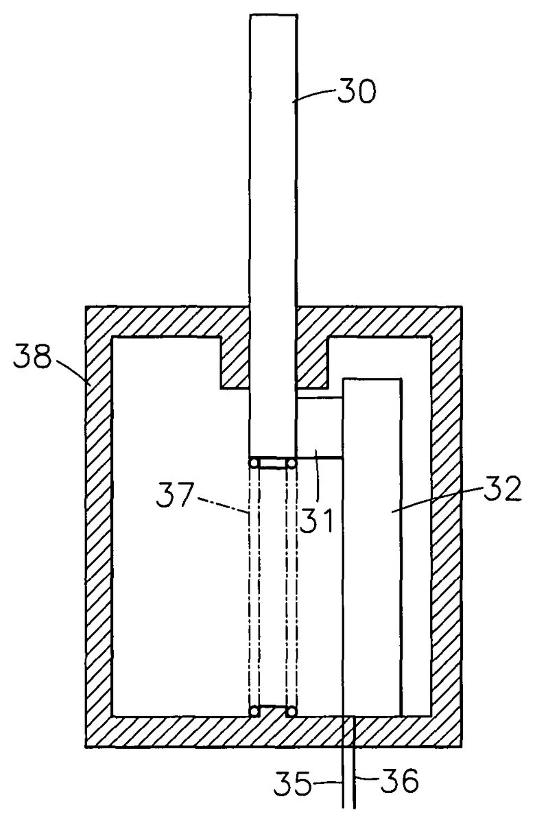
DETAILED DESCRIPTION OF THE INVENTION Referring toFIGS. 2A˜2D, a button30is shown having a contact31electrically disposed in contact with resistors33and34. The resistors33and34are installed in a stop member32at a circuit board15. The resistors33and34have lead wires35and36for connection to an external circuit. The button30is movable along the stop member32toward or apart from the circuit board15between an upper limit position as shown inFIGS. 2A and 2Band the lower limit position as shown inFIGS. 2C and 2D. The contact31is constantly kept in contact with the resistors33and34to output an analog signal. When the contact31is moved with the button30along the stop member32(the resistors33and34), the impedance of the resistors33and34is relatively changed subject to the elevational position of the contact31, and the analog signal outputted by the resistors33and34is relatively changed. Referring toFIG. 3, the aforesaid stop member32, resistors33and34are packaged in a package shell38. The button30is slidably mounted in the shell38and partially extending out of the top side of the package shell38, having its contact31suspending inside the package shell38. The lead wires35and36of the resistors33and34extend out of the package shell38for connection to an external circuit. Referring toFIG. 4, a control button40is vertically slidably mounted in a frame11and spaced above a circuit board15. The control button40has a bottom reflecting surface41corresponding to an optical transmitter42and an optical receiver43at a circuit board15below. The optical transmitter42is controllable to transmit light toward the bottom reflecting surface41. The optical receiver43is controllable to receive reflected light from the bottom reflecting surface41. By means of measuring the energy of the reflected light from the bottom reflecting surface41, the optical receiver43detects the position (operation status) of the control button40and outputs a corresponding output signal to the circuit board15for further control. The control button40is supported on spring means (not shown) that automatically returns the control button40after the control button is pressed. Referring toFIG. 5, this embodiment is substantially similar to the embodiment ...
DETAILED DESCRIPTION OF THE INVENTION
Referring toFIGS. 2A˜2D, a button30is shown having a contact31electrically disposed in contact with resistors33and34. The resistors33and34are installed in a stop member32at a circuit board15. The resistors33and34have lead wires35and36for connection to an external circuit. The button30is movable along the stop member32toward or apart from the circuit board15between an upper limit position as shown inFIGS. 2A and 2Band the lower limit position as shown inFIGS. 2C and 2D. The contact31is constantly kept in contact with the resistors33and34to output an analog signal. When the contact31is moved with the button30along the stop member32(the resistors33and34), the impedance of the resistors33and34is relatively changed subject to the elevational position of the contact31, and the analog signal outputted by the resistors33and34is relatively changed.
Referring toFIG. 3, the aforesaid stop member32, resistors33and34are packaged in a package shell38. The button30is slidably mounted in the shell38and partially extending out of the top side of the package shell38, having its contact31suspending inside the package shell38. The lead wires35and36of the resistors33and34extend out of the package shell38for connection to an external circuit.
Referring toFIG. 4, a control button40is vertically slidably mounted in a frame11and spaced above a circuit board15. The control button40has a bottom reflecting surface41corresponding to an optical transmitter42and an optical receiver43at a circuit board15below. The optical transmitter42is controllable to transmit light toward the bottom reflecting surface41. The optical receiver43is controllable to receive reflected light from the bottom reflecting surface41. By means of measuring the energy of the reflected light from the bottom reflecting surface41, the optical receiver43detects the position (operation status) of the control button40and outputs a corresponding output signal to the circuit board15for further control. The control button40is supported on spring means (not shown) that automatically returns the control button40after the control button is pressed.
Referring toFIG. 5, this embodiment is substantially similar to the embodiment shown inFIG. 4with the exception of the shape of the control button40and the use of a package shell38. According to this embodiment, spring means39is provided to hold the control button40in non-pressed position and to return the control button40to the non-pressed position after the control button40is pressed. Further, the optical transmitter42and the optical receiver43have the respective lead wires45and46respectively extend out of the package shell38and connected to an external circuit.
Referring toFIGS. 6A˜6C, a circuit board15is provided having a through hole18cut through the top and bottom walls thereof, and a frame11is spaced above the circuit board15at a distance to support a button50. The circuit board15has an optical transmitter52and two optical receivers53and53′ mounted thereon. The optical transmitter52is disposed on the top wall of the circuit board15at one side relative to the through hole18. The two optical receivers53and53′ are vertically arranged in a line at an opposite side relative to the through hole18. The button50is vertically slidably mounted in the frame11, having an encoder card51downwardly extending from its bottom side and aimed at the through hole18of the circuit board15. The encoder card51has a plurality of transverse slots54arranged in parallel at different elevations. When the button50is not pressed, the optical receivers53and53′ measure the light from the optical transmitter52directly. When the button50is pressed, the optical receivers53and53′ measure the light passing from the optical transmitter52through the transverse slots54of the encoder card51and output a corresponding analog signal. Alternatively, the optical receiver53can be omitted, i.e., only the optical receiver53′ is used. In this case, the encoder card51is made having only one slot55, which has a width gradually reducing in one direction (seeFIG. 6D). For example, the slot55can be made having a triangular shape.
Referring toFIGS. 7A˜7C, a button12is vertically movably mounted in a frame11and stopped at a hollow rubber cone13at a circuit board15. The hollow rubber cone13has a conical conducting member60fixedly mounted on the inside and spaced above a rectangular conducting track61(or circular conducting track63) on a circuit board15. When the user presses the button12, the button12gives a pressure to the hollow rubber cone13, forcing the conical conducting member60to contact the rectangular conducting track61(or circular conducting track63), thereby producing an analog output signal corresponding to the contact area between the conical conducting member60and the rectangular conducting track61(or circular conducting track63), i.e., corresponding to the pressure applied to the button12. The rectangular conducting track61(or circular conducting track63) has lead wires62(or64) electrically connected to other circuits on the circuit board15. Further, a package shell38may be mounted on the frame11to hold the hollow rubber cone13, the circuit board15, and the conical conducting member60on the inside (seeFIG. 8). Further, spring means37is mounted inside the package shell38to support the button12(seeFIG. 8). The spring means37automatically returns the button12after the button12is pressed.
Referring toFIG. 9A, a button12is vertically movably mounted in a frame11and stopped at a hollow rubber cone13at a circuit board15. The hollow rubber cone13has a conical conducting member70fixedly mounted on the inside and spaced above a carbon film71that is printed on a circuit board15. The carbon film71is electrically connected to an external circuit by lead wires72. When the user presses the button12, the button12gives a pressure to the hollow rubber cone13, forcing the conical conducting member70to contact the carbon film71. Subject to the pressure applied to the conical conducting member70through the button12against the carbon film71, the contact area between the conical conducting member70and the carbon film71is relatively changed, therefore the impedance of the carbon film71and the electric current passing through the carbon film71are also relatively changed (seeFIGS. 9B and 9C, providing a corresponding analog output signal indicative of the applied pressure.
FIG. 10is substantially similar toFIG. 9A. According to this embodiment, a package shell38is mounted on the frame11to hold the hollow rubber cone13, the circuit board15, and the conical conducting member70on the inside. Further, spring means37is mounted inside the package shell38to support the button12. The spring means37automatically returns the button12after the button12is pressed. The lead wires72extend out of the package shell38for connection to an external circuit.
Referring toFIGS. 11A and 11B, a circuit board23is provided having four resistors24arranged on the top wall thereof and spaced from one another at 90-degrees. A rubber member21is mounted on the top wall of the circuit board23over the area of the resistors24. The rubber member21comprises four bottom recesses27, four metal conducting portions22respectively fixedly mounted in the four bottom recesses27and respectively and vertically aimed at the resistors24, and four protruding portions26protruded from the top side corresponding to the metal conducting portions22. A cross button20is provided having a bottom center shaft28pivoted to the center of the rubber member21and four press button portions25equiangularly spaced around the border area corresponding to the protruding portions26. When biasing the cross button20, one press button portion25is forced against the corresponding protruding portion26to press the associating metal conducting portion22against the corresponding resistor24, producing an output signal indicative of the biasing direction of the cross button20and the pressured applied (seeFIGS. 11C˜11F). The technical features of this embodiment are applicable to a toggle switch (button).
Referring toFIG. 12, a circuit board23is provided having a resistor (not shown) on the top wall. A rubber member132is mounted on the circuit board23. The rubber member132has a bottom recess27, a metal conducting portion22fixedly mounted in the bottom recess27and aimed at the resistor of the circuit board23, and a protruding portion26protruded from the top side corresponding to the metal conducting portion22. A frame11is provided above the circuit board23to support a button30. The button30is vertically slidably mounted in the frame11, having a beveled bottom edge131facing the protruding portion26. By means of pressing the button30to force the beveled bottom edge131against the protruding portion26of the rubber member132, the metal conducting portion22is forced against the resistor at the circuit board, changing the impedance of the resistor, and therefore a corresponding output signal is produced.
FIG. 13shows a button structure substantially similar to the embodiment shown inFIG. 12with the exception that the button30has a flat bottom edge; the protruding portion26has a beveled top edge134facing the flat bottom edge of the button30.
Referring toFIG. 14, the button30can be made having a beveled bottom edge131; the rubber member132can be made having a beveled top edge134; the metal conducting portion133of the rubber member132at the circuit board23can be made having a beveled bottom edge135facing the resistor (not shown) at the circuit board23.
Referring toFIGS. 15A˜15D, a conducing track140may be used to substitute for the aforesaid resistor24. Subject to the contact area between the metal conducting portion22and the conducting track140, (i.e., subject to the pressure applied to the button), a corresponding output signal is produced.
Referring toFIG. 16A, the conducting track140has the conducting lines thereof electrically connected to an IC that reads in the pressure applied through the metal conducting portion22to the conducting track140.
Referring toFIG. 16B, the conducting track140has the conducting lines thereof electrically connected to resistor means that changes the impedance upon contact of the metal conducting portion22, thereby outputting a signal indicative of the pressure applied through the metal conducting portion22to the contact tract140.
Referring toFIG. 17A, the button structure comprises a circuit board23, two tin plates150arranged on the circuit board23, a resistor24connected between the two tin plates150, a rubber member132mounted on the circuit board23over the resistors24and the tin plates150, a metal conducting portion133fixedly mounted in the rubber member132and spaced above the resistor24. The metal conducting portion133has a beveled bottom edge135facing the resistor24. The resistor24according to this embodiment is an open-circuit resistor formed of a continual carbon film or continual resistor strip. The button structure according to this embodiment further comprises a frame (not shown) disposed above the rubber member132, and a button (not shown) vertically movably mounted in the frame and operable to press the rubber member132and to further force the metal conducting portion133against the resistor24. When the button is not pressed, the circuit of the resistor24and the two tin plates150is open. On the contrary, when the button is pressed to force the metal conducting portion133against the resistor24, the circuit of the resistor24and the two tin plates150is closed.
FIG. 17Bis substantially similar toFIG. 17Awith the exception of the shape of the metal conducting portion. According to this embodiment, the metal conducting portion133has a semispherical shape.
In general, a button structure for game controller in accordance with the present invention has the following features and advantages:
1. By means of changing the biasing angle of the button or the pressure applied to the button when pressing the button, the contact area between the metal conducting portion and the resistor or conducting track at the circuit board is relatively changed, and the value of the output signal is also relatively changed to give a corresponding control. The button structure can be made in a single module for easy and quick installation, saving much the cost.
2. The impedance of the resistor used in every resistor must checked to be within a predetermined tolerance value. By means of the use of a continual carbon film to substitute for a conventional resistor, the tolerance test is easy. Through only one single test is OK. When a conventional resistor is used, the tolerance test must be made at last twice.
3. Because of continual carbon films and continual resistor strips have the characteristic of low tolerance value, all buttons in a game controller according to the present invention show uniformity in triggering performance, i.e., when different buttons of the game controller produce approximately an equal value output when they receive a same pressure.
4. By means of the use of a continual resistor strip to substitute for a conventional non-continual resistor, the invention eliminates the drawback of the use of a conventional non-continual resistor strip. When a conventional non-continual resistor strip is used, the distance of the open circuit must be limited to a very small value to prevent electric leakage. When forming a non-continual resistor strip on a circuit board by printing, dispersion of printing material may occur. Either electrical leakage or dispersion of printing material may result in an error output, and an output signal may be produced erroneously when the button is not pressed. The invention eliminates these problems.
5. When a non-continual resistor strip is used, the positioning of the metal conducting portion must be accurately aimed at the open circuit area of the non-continual resistor strip to ensure accurate signal output upon pressing of the button. Because of the advantage of low positioning precision requirement, the use of a continual resistor strip to substitute for a conventional non-continual resistor strip greatly improves the yield rate of game controller.
6. When using a high sensitivity game controller, the game controller may be unable to define every instruction precisely because the area and elasticity of the finger pads of different users or the value of electrical charges carried in the finger pads of different users are different. Further, when playing an exciting game or shooting game, the sweat of the finger may cause a contact error. The invention controls the value of the output signal subject to the biasing angle of the button or the value of pressure applied to the button that controls the contact area between the metal conducting portion and the carbon film or conducting track, assuring high sensitivity and high reliability.
Although particular embodiments of the invention have been described in detail for purposes of illustration, various modifications and enhancements may be made without departing from the spirit and scope of the invention. Accordingly, the invention is not to be limited except as by the appended claims.
Claims
- A button structure used in a game controller, comprising: a rubber member mounted on a circuit board inside the game controller, said rubber member having a metal conducting portion disposed at a bottom side thereof;a continual resistor strip mounted in the circuit board carrying said rubber member and spaced below said metal conducting portion of said rubber member;a contact area produced upon contact between said rubber member and said continual resistor strip for causing said continual resistor strip to output a signal corresponding to the dimension of said contact area;and a button spaced above said rubber member and biasable to deform said rubber member and to further force said metal conducting portion into contact with said continual resistor strip.
- The button structure as claimed in claim 1 , wherein said continual resistor strip is a carbon film.
- The button structure as claimed in claim 1 , wherein said button has a bottom shaft pivoted to said rubber member.
- A button structure used in a game controller, comprising: a package shell formed of a part of said game controller;a printed circuit board mounted inside said package shell;a button mounted in said package shell and axially movable relative to said printed circuit board;drive means mounted on said button in a coaxial manner relative to said button and movable by said button;a continual resistor strip mounted in said printed circuit board;a contact area produced between said drive means and said continual resistor strip for causing said continual resistor strip to output a signal corresponding to the dimension of said contact area when said drive means is moved by said button, the dimension of said contact area between said drive means and said continual resistor strip determining the value of the signal outputted by said continual resistor strip.
- The button structure as claimed in claim 4 , wherein said continual resistor strip is a carbon film.
Disclaimer: Data collected from the USPTO and may be malformed, incomplete, and/or otherwise inaccurate.