U.S. Pat. No. 7,594,854
VIDEO GAME SYSTEM WITH DATA TRANSMITTING/RECEIVING CONTROLLER
AssigneeNintendo Co., Ltd.
Issue DateDecember 17, 2002
Illustrative Figure
Abstract
A game machine is provided with a controller control circuit including a data transfer control circuit. When the data in a first external RAM attached to a first controller is transferred to a second external RAM attached to a second controller, the data transfer control circuit transmits a predetermined command to the first controller. The data stored in the first external RAM is memorize through a data transfer control circuit. The data transfer control circuit then transmits a predetermined command to the second controller. In response thereto, the data stored in the internal RAM is transmitted to the second controller to be stored in the second external RAM.
Description
EMBODIMENT FIG. 2is an exemplary illustration showing a game machine system according to one illustrative embodiment of the present invention. The game machine system is, for example, a video game machine system, which inclusively comprises a game machine10, a ROM cartridge20(as one example of an external memory device), a monitor30(as one example of a display means) connected to the game machine10, a controller40(as one example of a player controller operating device), and a RAM cartridge50, as one example of an extension device detachably attached to the controller40. The external memory device stores image data and program data for image processing for games, and audio data for music, sound effects, etc. A CD-ROM or a magnetic disc may alternatively be employed in place of the ROM cartridge. Where the game machine system of this example is applied to a personal computer, an input device such as a keyboard or a mouse is used as the player operating device. FIG. 3is a block diagram of the game machine system of this example. The game machine10incorporates therein a central processor unit (hereinafter “CPU”)11and a bus control processing circuit12. The bus control processing circuit12is connected to a cartridge connector13for detachably attaching the ROM cartridge20, as well as a working RAM14. The bus control processing circuit12is connected to an audio signal generating circuit15for outputting an audio signal processed by the CPU11and a video signal generating circuit16for outputting a video signal, and further with a controller control circuit17for serially transferring operating data of one or a plurality of controller(s)40and/or data from RAM cartridge(s)50. The controller control circuit17is connected with controller connectors (hereinafter abbreviated as “connectors”)181-184which are provided at a front face of the game machine10. To the connector18is detachably connected a connection jack41and the controller40through a cable42. Thus, the connection of the controller to the connector181-184places ...
EMBODIMENT
FIG. 2is an exemplary illustration showing a game machine system according to one illustrative embodiment of the present invention. The game machine system is, for example, a video game machine system, which inclusively comprises a game machine10, a ROM cartridge20(as one example of an external memory device), a monitor30(as one example of a display means) connected to the game machine10, a controller40(as one example of a player controller operating device), and a RAM cartridge50, as one example of an extension device detachably attached to the controller40. The external memory device stores image data and program data for image processing for games, and audio data for music, sound effects, etc. A CD-ROM or a magnetic disc may alternatively be employed in place of the ROM cartridge. Where the game machine system of this example is applied to a personal computer, an input device such as a keyboard or a mouse is used as the player operating device.
FIG. 3is a block diagram of the game machine system of this example. The game machine10incorporates therein a central processor unit (hereinafter “CPU”)11and a bus control processing circuit12. The bus control processing circuit12is connected to a cartridge connector13for detachably attaching the ROM cartridge20, as well as a working RAM14. The bus control processing circuit12is connected to an audio signal generating circuit15for outputting an audio signal processed by the CPU11and a video signal generating circuit16for outputting a video signal, and further with a controller control circuit17for serially transferring operating data of one or a plurality of controller(s)40and/or data from RAM cartridge(s)50. The controller control circuit17is connected with controller connectors (hereinafter abbreviated as “connectors”)181-184which are provided at a front face of the game machine10. To the connector18is detachably connected a connection jack41and the controller40through a cable42. Thus, the connection of the controller to the connector181-184places the controller40into electric connection to the game machine10, enabling transmission and reception of data therebetween.
More specifically, the bus control processing circuit12inputs commands output as parallel signals from CPU11via a bus, performs parallel to serial conversion, outputs command as serial signals to the controller control circuit17, and converts serial signal data input from the controller control circuit17into parallel signals and output such signals to the bus. The data output through the bus is subject to processing by CPU11, or is stored in W-RAM14. The W-RAM14is a memory temporary storing data to be processed by CPU11, wherein read-out and write-in of data is possible through the bus control circuit12.
FIG. 4is a diagrammatic illustration showing memory regions assigned to respective memory spaces. The memory spaces accessible by the CPU via the bus control processing circuit12involves an external memory address space of the ROM cartridge20and a memory address space of the W-RAM14. The ROM cartridge20is structured by mounting on a board a ROM stored with data for game processing and accommodating the same board in a housing. The ROM storage data is shown by the external memory region shown inFIG. 4. The ROM includes an image data storage region201for storing image data required to cause the game machine10to generate image signals for the game, and a program data region202for storing program data required for predetermined operation of the CPU11. In the program data region202, there are stored an image display program for performing image display processing based on image data201, a time-measuring program for carrying out measurement of time, and a determination program for determining that the cartridge20and an extension expansion device50, are in a predetermined relationship. The details of the time-measuring program and the determination programs are described below. The memory region of W-RAM14includes a controller data region141for temporarily storing data representative of an operating state from a control panel.
FIG. 5is a more detailed circuit diagram of a controller control circuit17. The controller control circuit17transmits and receives data in serial form to and from the bus control processing circuit12and the controller connectors181-184, and includes a data transfer control circuit171, a signal transmitting circuit172, a signal receiving circuit173and a RAM174for temporarily storing transmission and reception data. The data transfer control circuit171includes a parallel-serial conversion circuit and a serial-parallel conversion circuit for conversion of data format during data transfer, and also performs control of write-in and read-out of the RAM174. The above-mentioned serial-parallel conversion circuit converts serial data supplied from the bus control processing circuit12into parallel data to provide such data to the RAM174or the signal transmitting circuit172. The parallel-serial conversion circuit converts parallel data supplied from the RAM174or the signal receiving circuit173into serial data to provide such data to the bus control processing circuit12. The signal transmission circuit172converts parallel data for signal read-in control of the controller40supplied from the data transfer control circuit171and write-in data (parallel data) to the RAM cartridge50into serial data, which serial data is transmitted through a corresponding channel CH1-CH4to each of the plurality of controllers40. The signal receiving circuit173receives serial read-out data, representative of an operating state of each of the controller40, input through a corresponding channel CH1-CH4to each of the controller40as well as read-out data from the RAM cartridge50, to convert such data into parallel data to provide it to the data transfer control circuit171.
The signal transmitting circuit172and the signal receiving circuit173in the exemplary embodiment adopt a duty-cycle modulation and demodulation (hereinafter referred to as “modulation/demodulation”) method as one example of the modulation/demodulation method that may be employed here. The duty-cycle modulation/demodulation method, as shown inFIG. 6, is a modulation/demodulation method wherein “1” and “0” are represented by varying a Hi time period and a Lo time period for a signal at a certain interval. Explaining the modulation/demodulation method in more detail, when data to be transmitted in serial is a logical “1”, a signal having, within one cycle period T, a high-level period tH rendered longer than a low-level period tL (tH>tL) is transmitted. When data to be transmitted is a logical “0”, a signal having, within one cycle period T, tH rendered shorter than tL (tH<tL) is transmitted.
The demodulation method includes sampling on a serial signal received (bit transmission signal) to monitor at all times whether the received signal is at a high level or a low level, wherein one cycle is expressed as T=tL+tH, where the time period of low till change to high is tL and time period of high till change to low is tH. In this case, the relationship of tL and tH being tL
The RAM174includes memory regions or memory areas174a-174has shown in a memory map ofFIG. 7. Specifically, the area174astores a command for channel1, while the area174bstores transmission data and reception data for channel1. The area174cstores a command for channel2, while the area174dstores transmission data and reception data for channel2. The area174estores a command for channel3, while the area174fstores transmission data and reception data for channel3. The area174gstores a command for channel4, while the area174hstores transmission data and reception data for channel4.
Accordingly, the data transfer control circuit171operates to write-in control to the RAM174data transferred from the bus control processing circuit12or operating state data of the controller40received by the signal receiving circuit173or read-out data from the RAM cartridge50, and read data out of the data174based on a command from the bus control circuit12to transfer it to the bus control processing circuit12.
With referring toFIG. 8andFIG. 9, the controller of this embodiment shown includes a housing401consist of an upper half and a lower half At both left and right ends of the housing401, a left grip402L and a right grip402R are respectively formed in a manner that the same are protruded toward a front side. In an intermediate position between the left grip402L and the right grip402R, a center grip402C is formed in a manner that the same is protruded toward the front side. A cross-direction designation switch403which is a digital joystick is formed on a surface of the housing401in the vicinity of a base end of the left grip402L. Action designation switches404A,404B,404C,404D,404E and404F which designate six (6) kinds of actions are respectively formed on the surface of the housing401in the vicinity of a base end of the right grip402R.
An analog joystick45which is capable of designating all directions within 360 degrees is formed on the housing401in the vicinity of a base end of the center grip402C. At an approximately central position of the housing401, a start switch405which designates a start of a game is formed. Furthermore, the start switch405is positioned at an approximately center of an area surrounded by the switches403and404A to404F, and the analog joystick45.
Furthermore, a pair of side surface switches406L and406R are formed on a rear surface of the housing401, and a bottom surface switch407is formed at an approximately center of the lower half in the vicinity of the base end of the center grip402C.
A rear surface of the lower half is extended toward direction of a bottom surface, and an opening portion408is formed at a tip end thereof. In an interior of the opening portion408, a connector (not shown) to which an expansion cartridge50shown inFIG. 4is connected is provided. Furthermore, a lever409for discharging the cartridge50inserted into the opening portion408is formed at a position of the opening portion408. In addition, at a side opposite to the lever of the opening portion408to which the above described expansion cartridge50is inserted, a notch410is formed, and the notch410secures a space for withdrawing the expansion cartridge50in discharging the expansion cartridge50with utilizing the lever409.
Now, with referring toFIG. 10toFIG. 13, the analog joystick45will be described in detail. The analog joystick45is constructed as a joystick unit as shown inFIGS. 10 to 13. The joystick unit is sandwiched by the upper half and the lower half of the housing401. The joystick unit includes a housing formed by a case451and a cover452, and an inner case453are accommodated within the housing.
As shown inFIG. 11andFIG. 12, the inner case453includes a bowl-shaped recess portion454formed at a center of the inner case453, and two pairs of support plates455aand455b, and456aand456bare provided around the recess portion454with angle-interval of 90 degrees, and semicircular bearings457aand457b, and458aand458bare formed on the support plates455aand455b, and456aand456b, respectively. The bearings457aand457bor458aand458bare arranged on the same axis line, and axes of the bearings457aand457b, and458aand458bare at the same height level, and orthogonally intersect each other. Wheels459and460having rotation shafts which orthogonally intersect each other are rotatably supported at a side surface of the inner case453, and gears461are uniformly formed on the respective wheels459and460.
The analog joystick unit further includes swingable members462and463. One swingable member462is formed by an arc-like member which is provided with a long hole464being made long in a longitudinal direction of the arc-like member, and supporting shafts465aand465bare formed at both ends of the swingable member462, and shaft end portions467aand467brespectively having flat surfaces466aand466bare extended from the supporting shafts465aand465b, and a sector gear468is provided on one shaft end portion467b. The other swingable member463is different from the one swingable member462in that the swingable member463is constructed by an arc-like member having a radius of curvature smaller than that of the swingable member462; however, in other aspects, the swingable member463is constructed in a manner similar to or the same as the swingable member462. That is, a reference numeral469denotes a long hole, reference numerals470aand470bdenote supporting shafts, reference numerals471aand471bdenote flat surfaces, reference numerals472aand472bdenote shaft end portions, and a reference numeral473denotes a sector gear.
The supporting shafts465aand465b, and470aand470bare individually inserted into the two sets of bearings457aand457b, and458aand458bof the inner case453, and therefore, the part of the swingable members462and463can be supported in a swing-free fashion, and the swingable members462and463are arranged so that the longitudinal directions of the long holes464and469orthogonally intersect each other and are overlaid with an interval or gap. In the pair of swingable members462and463thus attached to the inner case453, the sector gears468and469engage the above described gears461. Furthermore, respective ones of the above described flat surfaces466aand466b, and471aand471bare included in the same horizontal plane in a neutral state of a lever474(described later).
As shown inFIG. 12, the lever474includes protrusions475which protrude toward outer radius directions at one end of the lever474, and a ball portion476at a middle portion of the lever474, and a connection portion477at the other end of the lever474. Grooves478which extend in a latitude direction at positions apart from each other by 180 degrees are formed on the above described ball portion476. The diameter of the lever474is selected at a size which is not larger than the sizes of the short directions of the long holes464and469formed on the swingable members462and463. Preferably, the diameter of the lever474is selected at a size by which the lever474can be slidably inserted into the long holes464and469without shaking. Then, the one end portion of the lever474penetrates through the long holes464and469, and the protrusions475fit into the long hole464of a lower side swingable member462. Therefore, the protrusions475of the lever474are arranged to be protruded in a direction orthogonally intersected to the longitudinal direction of the long hole469of an upper swingable member463being attached to the inner case453, and therefore, if the lever474is pulled-up, the protrusions475are prevented from-being slipped-off by the upper swingable member463.
A mechanical structure portion assembled as shown inFIG. 11is accommodated within the outer case451shown inFIG. 10. At this time, the inner case453is fixed to the outer case451by a suitable means such as screws (not shown).
Then, as well seen fromFIG. 12there are provided on the inner case453photo-interrupters479and480which are opposite to the two wheels459and460. The photo-interrupters479and480respectively include light-emitting elements and light-receiving elements (both not shown), and lights emitted by the light-emitting elements are received by the light-receiving elements through slits481and482respectively formed on the wheels459and460. Therefore, the photo-interrupters479and480respectively detect the slits481and482, and in response to the slits481and482, outputs pulse signals according to rotations of the wheels459and460.
In addition, the height level of swing-shafts (supporting shafts465and470) of the swingable members462and463are coincident with a height level of a center of the ball portion476of the lever474. Furthermore, a printed-circuit board (not shown) to which a flexible wiring plate483is connected is assembled in the outer case451, and the light-emitting elements and the light-receiving elements included in the photo-interrupters479and480are electrically connected to printed patterns of the board.
As shown inFIG. 13, a grooved ring484is supported above the flat surfaces466and471provided on the pair of swingable members462and463, and a coil spring485is arranged above the grooved ring484. The grooved ring484is one example of a pushing-down member, and in the neutral state of the lever474, a lower surface of the ring484becomes in horizon, and the lower surface of the ring484and the above described flat surfaces466and471are brought into surface-contact with each other.
As shown inFIG. 13, a guide ring486is attached to the cover452, and a circular hole487is formed at a center portion of the guide ring486. The guide ring486further includes a guide wall488which is a rising slope raised from an inner periphery defining the hole487toward an outer periphery of the guide ring486. That is, the guide wall488is formed as a whole in “an earthenware mortar” or “cone”-shape. Then, in viewing the guide wall488from above, the guide wall488has an outer edge491which becomes octagonal as seen from the above.
In addition, a diameter of the hole487is selected to a size that is the same or approximately the same as a diameter of an outer peripheral surface of the ball portion476of the above described lever474. Therefore, as shown inFIG. 13, the inner edge defining the hole487is brought into contact with the ball portion476of the lever474, and therefore, the lever474is supported by the ball portion476and the hole487in a manner that the lever474can be swung or inclined in any direction. Furthermore, circular bosses489are formed at two positions apart from each other by 180 degrees on the inner edge defining the hole487of the guide ring486in a manner that the bosses489protrude toward an inner radius direction of the hole487, and the bosses489individually fit into the grooves478formed in the latitude direction of the above described ball portion476. Therefore, the lever474can be swung around an axis of the bosses489, but the lever474can not be rotated around the axis of the lever474itself. Therefore, the lever474is prevented from being rotated around its axis by the grooves478of the ball portion476and the bosses489.
Furthermore, if the cover452is attached to the case451, a spring490is sandwiched and compressed between the grooved ring484and the cover452. Therefore, the flat surfaces466and471of the pair of swingable members462and463are always depressed by a force of the spring490via the grooved ring484, and by such a depression force, the pair of swingable members462and463are always elastically biased so that attitude of both members462and463is not in any direction, and therefore, the lever474has a vertical attitude, that is, the lever474is always elastically biased into its neutral state.
The lever474is provided with an operating knob492which is attached to the lever474via the connection portion477. On an upper surface of the operating knob492, a recess portion493is formed such that a finger of the hand can easily put on the knob492.
In the above described analog joystick unit, according to an inclined direction and an inclined angle of the lever474, the swingable members462and/or463are swung, and then, the wheels459and/or460are rotated in accordance with the inclined angle of the swingable members462and/or463, and therefore, pulses according to rotation amounts of the wheels459and/or460are outputted, and the pulses are utilized as coordinate signals in an X axis and/or a Y axis directions.
FIG. 14is a detailed circuit diagram of a controller40and a RAM cartridge50(as one example of an extension device). The controller40incorporates within its housing, electronic circuits such as an operation signal processing circuit44, etc. in order to detect operating states of the switches403-407or the joystick45or the like and transfer detected data to the controller control circuit17. The operation signal processing circuit44includes a signal receiving circuit441, a control circuit442, a switch signal detecting circuit443, a counter444, a signal transmitting circuit445, a joyport control circuit446, a reset circuit447and a NOR gate448.
The signal receiving circuit441converts a serial signal, such as a control signal transmitted from the controller control circuit17, write-in data to the RAM cartridge50, etc., into a parallel signal to supply it to the control circuit442. The control circuit442generates a reset signal to cause resetting (e.g., setting to 0) on measured values of an X-axis counter444X and a Y-axis counter444Y included in the counter444, when the control signal transmitted from the controller control circuit17is a reset signal for an X, Y coordinate of the joystick45. The joystick45includes photo-interrupters for the X-axis and Y-axis so as to generate the number of pulses proportional to the amount of inclination of a lever in directions of X-axis and Y-axis, providing respective pulse signals to the counters444X and444Y. The counter444X, when the joystick45is inclined in the X-axis direction, measures the number of pulses generated in proportion to the amount of inclination. The counter444Y measures the number of pulses generated in proportion to the amount of inclination, when the joystick45is inclined in the Y-axis direction. Accordingly, the resultant vector, determined by the measured values in X-axis and Y-axis of the counter444X and the444Y, determines the direction of movement and the coordinate position for the heroic character or the cursor. The counter444X and the counter444Y are also reset of their measured values by a reset signal supplied from the reset signal generating circuit447upon turning on the power supply, or a reset signal supplied from the switch signal detecting circuit443when the player depresses simultaneously two switches previously determined.
The switch signal detecting circuit443responds to an output command signal representing a switch state supplied at a constant period (e.g., at a 1/30-second interval as a frame period of a television), and reads a signal that is varied by the state of depression of the cross switch403and the switches404A-404F,405,406L,406R and407to supply it to the control circuit442.
The control circuit442responds to a read-out command signal of operating state data from the controller control circuit17, and supplies the operating state data of the switches403-407and the measuring values of the counters444X,444Y to the signal transmitting circuit445in a predetermined data-format order. The signal transmitting circuit445converts these parallel signals output from the control circuit442into serial data to transfer them to the controller control circuit17via a conversion circuit43and a signal line42.
The control circuit442is connected to an address bus, a data bus, and a port control circuit446through a port connector. The port control circuit446performs input-output control (or signal transmission or reception control) on data according to commands by the CPU11, when the RAM cartridge50(as one example of an extension device) is connected to a port connector46. The RAM cartridge50includes a RAM51connected to the address bus and the data bus and a battery52connected thereto for supplying power source to the RAM51. The RAM51is a RAM that has a capacity lower than a half of a maximum memory capacity accessible by using an address bus, and is comprised, for example, of a 256 k-bit RAM. The RAM51stores backup data associated with a game, so that, if the RAM cartridge50is removed out the port connector46, the stored data is kept by receiving power supply from the battery52.
FIG. 15is a graphical illustration of a data format by which the game machine or image processing apparatus reads out data representative of an operating state of switches403-407and joystick45from the controller40. The data generated by the controller40is configures as 4-byte data. The first-byte represents B, A, G, START, upper, lower, left and right, i.e., represents the depression of the switch404B,404A,407,405and the four cross switch403directions. For example, when the button B, i.e., the switch404B, is depressed, the highest order bit of the first byte becomes “1”. Similarly, the second-byte represents JSRST, 0 (not employed in the embodiment), L, R, E, D, C and F, i.e., the depression of the switch409,406L,406R,404E,404D,404C and404F. The third byte represents by binary digit the X coordinate value (the value measured by the X counter444X) dependent upon the inclination angle of the joystick45in the X direction. The fourth byte represents by binary digit the Y coordinate value (the value measured by the Y counter444Y) which value is dependent upon the inclination angle of the joystick45in the Y direction. Because the X and Y coordinate values are expressed by 8 bits of binary digits, the conversion into decimal digits makes it possible to represent the inclination of the joystick45by a numeral from 0-225. If the highest order bit is expressed by a signature denoting a negative value, the inclination angle of the joystick45can be expressed by a numeral between −128 and 127.
FIG. 16shows an embodiment wherein an extension device60including an LCD (Liquid Crystal Display)62and an LCD controller61is connected to a controller40. In this embodiment, when the extension device60is connected to the connector46, the LCD controller61is electrically connected to the joy port control circuit446to be enabled to transmit and receive data. The LCD controller61outputs an image signal to the LCD62based on data outputted from the joy port control circuit46. The LCD62displays an image picture in accordance with the image signal from the LCD controller61.
Incidentally, although the extension device50including the RAM and the extension device60including the LCD62were employed, it is possible to utilize an arbitrary extension device that is adapted to transmit and/or receive data to operate.
Explanation is next made as to transmission and reception of data between the game machine10and the controller40.
Referring first to a flowchart for the CPU of the game machine10inFIG. 17, explanations will be made on image processing. At a step S11, the CPU11is initialized based on an initial value (not shown) stored in the program data area202inFIG. 4. Then, at a step S12, the CPU11outputs a control pad data request command stored in the program data area202to the bus control circuit12. At a step S13, the CPU11carries out the desired image processing based on the program stored in the program data area202and the image data area201. While the CPU11is executing step S13, the bus control processing circuit12is executing steps S21-S24. Then, at a step S14, the CPU11outputs image data based on the control pad data stored in the control-pad data area141inFIG. 4. After completing step S14, the CPU branches to steps S12and repeats the execution of steps S12-S14.
The operation of the bus control processing circuit12is explained in conjunction withFIG. 18. At a step S21, the bus control circuit12determines whether or not the CPU11has output a controller data request command (a request command for data relating to the switches of the controller40or data on the extension device50). If a controller data request command has not been output, the processing circuit12waits until one is output. If a controller data request command has been outputted, the process proceeds to a step S22. At the step S22, the bus control circuit12outputs a command for reading in data of the controller40(command 1 or command 2 referred to above) to the controller control circuit17. Then, at a step S23, the bus control circuit12determines whether or not the controller control circuit17has received data from the controller40to store it in the RAM174. If the controller control circuit17has not received data from the controller40to store in the RAM174, the bus control circuit12waits at step S23. If the controller control circuit17has received data from the controller40to store in the RAM174, the process proceeds to a step S24. At step S24, the bus control circuit12transfers the data of the controller40stored in the RAM174to the W-RAM14. The bus control circuit12, when completing the data transfer to the W-RAM14, returns the process back to the step S21to repeat execution of the step S21—the step S24.
TheFIG. 17andFIG. 18flowcharts show the example wherein, after the bus control circuit12has transferred data from the RAM174to the W-RAM14, the CPU11processes the data stored in the W-RAM14. However, the CPU11may directly process the data in the RAM174through the bus control circuit12.
FIG. 19is a flowchart for explaining the operation of the controller control circuit17. At a step S31, it is determined whether there is data to be written by the bus control circuit12. If there is not, the data transfer control circuit171waits until there is data to write-in from the bus control circuit12. If there is data to be written, at a next step S32the data transfer control circuit171causes the RAM174to store commands for the first to the fourth channels and/or data (hereinafter abbreviated as “command/data”). At a step S33, the command/data for the first channel is transmitted to the controller40being connected to the connector181. The control circuit442performs a predetermined operation based on the command/data to output data to be transmitted to the game machine10. The content of the data will be described below in explaining the operation of the control circuit442. At a step S34, the data transfer control circuit171receives data output from the control circuit442, to cause the RAM to store the data.
At a step S35the command/data for the second channel is transmitted to the controller40, in a manner similar to the operation for the first channel at the steps S33and S34. The control circuit442performs a predetermined operation based on this command/data to output the data to be transmitted to the game machine10. At a step S36data transfer and write-in processes are carried out for the second channel. Meanwhile, at a step S37, the command/data for the fourth channel is transmitted to the controller40. The control circuit442performs a predetermined operation based on this command/data to output the data to be transmitted to the game machine10. At a step S38data transfer and write-in processes are carried out for the third channel. Furthermore, at a step S39, the command/data for the fourth channel is transmitted to the controller40. The control circuit442of the controller40performs a predetermined operation based on this command/data to output the data to be transmitted to the game machine10. At a step S40data transfer and write-in processes are carried out for the fourth channel. At a subsequent step S41, the data transfer circuit171transfer in batch the data which have received at the steps S34, S36, S38and S40to the bus control circuit12.
In the above-identified manner, the data for the first channel to the fourth channel, that is, the commands for the controllers40connected to the connectors181-184and the operating state data to be read out of the controllers40, are transferred by time-divisional processing between the data transfer control circuit171and the control circuit442respectively within the controllers40.
FIG. 20is a flowchart explaining the operation of the controller circuit44. First, at a step S51, it is determined whether or not a command has been input from the image processing circuit10to the control circuit442. If no command has been inputted, the controller circuit waits for a command. If a command is input, at a step S52it is determined whether or not the command inputted to the control circuit442is a status request command (command “0”). If a command “0” is detected, the process proceeds to a step S53, wherein a status transmitting process is carried out.
At the step S53, where the CPU11outputs the command “0”, the data in the format as shown inFIG. 13is transmitted and received between the game machine10and the controller40. On this occasion, the control circuit442, when receiving the command “0” data configured by 1 byte (8 bits), transmits TYPE L (1 byte), TYPE H (1 byte) and the status. Here, TYPE L and TYPE H are data for identifying the function of a device or apparatus being connected to the joyport connector46, which are inherently recorded in the RAM cartridge50. This make possible recognition by the game machine10as to what extension device (e.g., a RAM cartridge50or other extension devices such as a liquid crystal display) is connected to the controller40. The status is data representative of whether or not an extension device such as a RAM cartridge50is connected to the port and whether or not the connection of the extension device is after resetting.
On the other hand, at the step S52if the determination reveals that there is not a command “0”, it is determined at a step S54whether or not the inputted command is a pad-data request command (command “1”). If it is a command “1”, the process proceeds to a step S55where the process of transmitting pad data is performed. Specifically, where the CPU11outputs a command “1”, the data in format as shown inFIG. 14is transmitted and received between the game machine10and the controller40. On this occasion, the control circuit442, if receiving command “1” data configured by 1 byte (8 bits), transmits the data of 14 switches (16 bits) of B, A, G, START, upper, lower, left, right, L, R, E, D, C and F, the data of JSRST (1 bit); and the data of the counter444X and the counter444Y (16 bits). By transmitting these data to the game machine10, the game machine10recognizes how the operator operated the controller40. Thus, these data are utilized for modifying the image by the game machine10in accordance with the operating state of the controller40as manipulated by the player.
At the foresaid step S54, if the determination reveals that there is not a command “1”, it is determined at step S56whether or not the input command is a read-out request command (command “2”) for data associated with the RAM cartridge50to be connected to the extension connector. If it is a command “2”, the process proceeds to a step S57where the process of reading out of the extension connector is performed. Specifically, where the CPU11outputs a command “2”, the data in format as shown inFIG. 13is transmitted and received between the game machine10and the controller40. On this occasion, when the control circuit442receives command “2” data configured by 1 byte (8 bits), address H representative of the higher-order bits (8 bits) of address, address L representative of the lower-order bits (3 bits) of address, and address CRC (5 bits) for checking for error in address data transmitted and received, the control circuit442transmits data stored in the RAM cartridge (32 bytes) and CRC (8 bits) for checking for data errors. In this manner, the connection of the RAM cartridge50(or other extension devices) and the game machine10enables the game machine10to process data from the RAM cartridge50, etc.
At the aforesaid step S56, if the determination is not a command “2”, it is determined at a subsequent step S58whether or not the inputted command is write-in request command (command “3”) for information associated with the RAM cartridge50being connected to the extension connector46. Where it is the command “3”, the process of data read-out is carried out at a step S59for the RAM cartridge50being connected to the extension connector46. Specifically, if the CPU11outputs a command “3”, the data shown inFIG. 23is transmitted and received, in response to the command “3”, between the game machine10and the controller40.
That is, when the control circuit442receives command “3” data configured by 1 byte (8 bits), address H representative of the higher-order bits of address (8 bits), address L representative of the lower-order bits of address (3 bits), address CRC for checking for error in address data transmitted and received (5 bits), and data to be transmitted to the RAM cartridge50(32 bytes), it transmits CRC for checking for error for data received (8 bits). In this manner, the connection of the extension device50and the game machine10enables the game machine10to control the extension device50. The connection of the extension device50and the game machine10also drastically improves the function of the controller40.
If at the aforesaid step S58the determination is not a command “3”, it is determined at a step S60whether or not it is a reset command (command255). Where it is the reset command (255), the process of resetting the counter444for the joystick45is performed at step S61.
Where the CPU11outputs a reset command (command255), the data shown inFIG. 25is transmitted and received between the game machine10and the controller40. That is, the control circuit442of the controller40, if receiving command255data configured by 1 byte (8 bits), outputs a reset signal to reset the X counter444X and counter444Y and transmits aforesaid TYPE L (1 byte), TYPE H (1 byte) and the status.
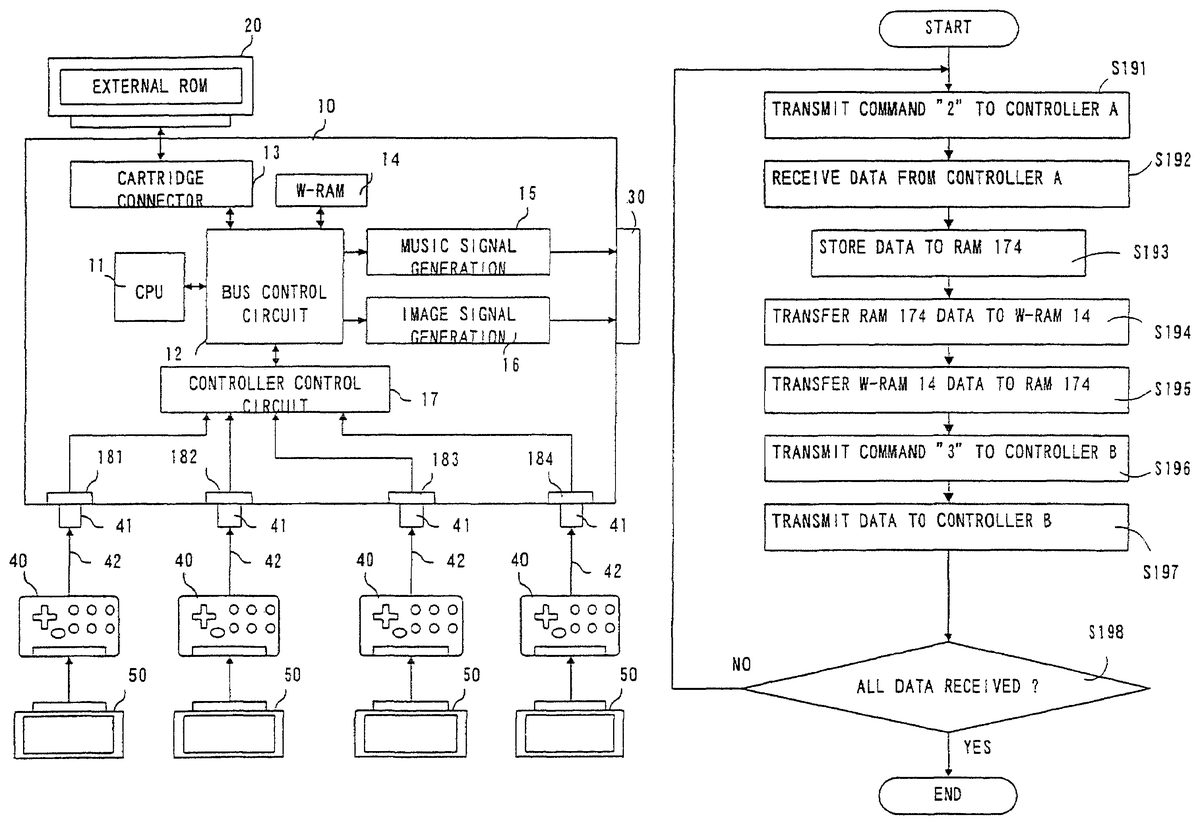
The operation by the controller control circuit17of transferring data will be explained using the flowchart inFIG. 26, wherein the data, stored in a RAM51within an extension device50connected to a joy port connector46of a controller40(controller A) having a connection jack41connected to the controller connector181is transferred to a RAM51within an extension device50connected to a joy port connector46of a controller (controller B) having a connection jack41connected to the controller connector182.
First, if the operator operates the controller40to determine commencement of backup or if the start of a copying operation is determined by the program, the data transfer control circuit171transmits a command “2” to the controller A at a step S191. The controller A performs a predetermined operation in accordance with the command “2” to transfer the data stored in the RAM51to the data transfer control circuit171. At a step S193, the data transfer control circuit171stores the data received from the controller A to the RAM174. At a step S194the data transfer control circuit171transfers the data stored in the RAM174to the W-RAM14. When the data format is different between the RAM51connected to the controller A and the RAM51connected to the controller B, the data stored in the W-RAM14is altered by the CPU11. At a step S195the data transfer control circuit171transfers the data stored in the W-RAM14to the RAM174. At a step S197, the data transfer control circuit171transmits a command “3” to the controller B. At a step S196, the data transfer control circuit171transmits the data stored in the RAM174to the controller B. At a step S198, it is determined whether or not the data to be transferred from the controller A to the controller B have all been transferred. If the transfer is completed, the backup operation is ended. Where the transfer is not completed, the step S191through the step S198are executed again.
By executing the step S191through the step S198in this manner, it is possible to store the data stored in the RAM51of the extension device50connected to the controller A to the RAM51of the extension device50connected to the controller B.
By so doing, it is possible to analyze a competition record of a competitor for future battle references. Even when a racing game or a baseball game is played alone, it is possible to compete with a competitor's machine or baseball team by using machine tuning data or baseball team data of a competitor.
A detailed operation for resetting the joystick45will be described next.
In order to reset the joystick45to determine an origin point thereof, there are three methods, i.e., a method through button operation, a method through turning-on/off the power source, and a method controlled by the image processor10.
(1) A reset operation by operating the buttons.
With reference to the flowchart shown inFIG. 27, a reset operation is shown for the counter444which stores data indicative of an inclined state of the joystick45, First, in a step S432, the switch signal detection circuit443detects whether or not the buttons406Lb406R and405are simultaneously depressed. Then, if the three buttons are not depressed, the detection of the switch signals is performed continuously. Furthermore, if the three buttons are simultaneously depressed, the reset signal is outputted.
In response to the reset signal, in a step S434, the count values of the X counter444X and the Y counter444Y are reset. Therefore, the origin point of the joystick is determined at every time that, for example, the buttons406L,406R and405are simultaneously depressed.
In this embodiment, at a time that the buttons406L,406R and405are simultaneously depressed by the operator, the reset signal is generated by the switch signal detection circuit443; however, the number of the buttons is not limited to three (3), and may, for example, be two (2) or four (4). Furthermore, buttons simultaneously depressed are not limited to the above described buttons, and may be arbitrary buttons.
(2) A reset operation by turning-on/off the power source.
With referring to a flowchart shown inFIG. 28, another reset operation of the counter444will be described. A reset signal is output from a power-on reset circuit447in response to the power source switch (not shown) of the image processor10being turned-on by the operator when the controller40is connected to the image processor10, or in response to a fact that the power source is supplied to the controller40by inserting the connection jack of the controller40into one of the controller connectors181-184of the image processor10when no controller40is connected to the image processor10. In response to such a reset signal, in a step S442, the count values of the X counter444X and the Y counter444Y are reset. Therefore, the origin point of the joystick is determined at every time that the power source is supplied to the controller40.
(3) A reset operation by the image processor10.
The counter444is also reset by executing the steps S60and S61shown in the above describedFIG. 20. Through such a reset operation, it is possible to freely determine the origin point of the joystick45by the program in accordance with a processing status of the image processor10.
According to the above described methods, it is possible to reset the X counter444X and the Y counter444Y. If the reset signal is output at a time that the lever474is in its neutral position, that is, at a time that the lever474is not operated by the operator, it is possible to prevent erroneous count values from being stored in the X counter444X and the Y counter444Y, and therefore, it is possible to prevent the erroneous count values from being transmitted to the image processor10.
Next, one example where the monitor screen is changed using the controller40will be described with referring toFIG. 29. A left illustration inFIG. 29shows the physically inclined amount of the lever474using orthogonal X-Y coordinates. More specifically, a circle illustrated at a center indicates the lever474, and in this illustration, a state where the operator does not operate the lever474, that is, a state where the lever474stands upright with respect to the housing. If the lever474is inclined toward a front side, the circle is moved in a +(positive) direction in the Y axis, and if the lever474is inclined toward a rear side, the circle is moved in a −(negative) direction of the Y axis. Furthermore, if the lever474is inclined toward a right direction, the circle is moved in a +(positive) direction of the X axis, and if the lever474is inclined toward a left side, the circle is moved in a −(negative) direction of the X axis.
A right illustration inFIG. 29shows a display screen of a game where an enemy34is aimed by inclining the lever474toward front, rear, left and right so as to move an aiming device35toward upper, lower, left and right. Clouds31, mountains32and buildings33constitute a background image which can be changed by, for example, scrolling, the enemy34is an object which can freely move within the screen. For example, when the enemy34is displayed in a right upper portion of the screen, if the operator inclines the lever474toward right and then front, the X counter444X and the Y counter444Y are both incremented, and thus, the count values thereof become larger. The count values are transmitted to the image processor10which changes a display position of the aiming device35thereby utilizing the data of the count values. Therefore, the aiming device35becomes to be super-positioned on the enemy34. Then, at a timing the aiming device35is just super-positioned on the enemy34, if the button such as the button404A is depressed, the switch data of the button is also transmitted to the image processor10similar to the counter data. Accordingly, the image processor10generates the image signal so as to display a missile (not shown) or the like which can attack the enemy34on the screen.
Next, one example of a case where the analog joystick is reset in a state where the lever474is deviated from the center, that is, the lever474is inclined will be described with reference toFIG. 30.
When the X counter444X and the Y counter444Y are reset at the coordinate position indicated by a solid circular line in a left illustration inFIG. 30, if the operator releases his or her hand from the lever474, the lever474returns to the center of the coordinate, i.e., a position indicated by a dotted circular line. A change of the image will be described with utilizing a right illustration inFIG. 30. First, when the X counter444X and the Y counter444Y are reset, as similar to the right illustration inFIG. 29, the aiming device35is displayed at the solid circular line because the count values of the X counter444X and the Y counter444Y are both “0” equal to the initial values. Next, if the operator releases his or her hand from the lever474, the lever474returns to the center position of the coordinate, and the X counter444X within the controller40is incremented and the Y counter444Y is decremented, and therefore, the count values of the counters444X and444Y become larger and smaller, respectively. The count values are transmitted to the image processor10which changes the display position of the aiming device35with utilizing the data of the count values to the position of an aiming device35indicated by a dotted line.
A description will be made of such a reset operation which is performed at a certain point in time. For example, if the operator presumes the position that the enemy34appears is the position of the aiming device35shown by the dotted line in the right illustration inFIG. 30, the operator wishes to super-position the aiming device35at the position of the dotted line aiming device35at an instance that the enemy34appears. However, if the aiming device35is continuously kept on the dotted line aiming device35, the operator who is a game player will be bored, and there is a further possibility that if the enemy34appears at a place not presumed, the operator cannot attack the enemy, and therefore, in order to super-position the aiming device35on the position of the dotted line aiming device35at an instance that the enemy34appears, and to freely move the aiming device35to other places, the above described reset function is used. In describing an action of the operator more specifically, the operator first inclines the lever474such that the aiming device35is displayed at a position symmetrically corresponding to the position presumed that the enemy34will appear (the position of the dotted line aiming device35) with reference to the solid line aiming device35. At that time, the physical coordinate position of the lever474becomes the solid circular line in the left illustration inFIG. 29. Then, the operator, for example, simultaneously depresses the three buttons of the buttons406L,406R and405. In response to the depression, the X counter444X and the Y counter444Y are both reset, and the aiming device35is displayed at the position of the solid line aiming device35. Then, the operator freely moves the aiming device35, and waits for an appearance of the enemy34. If the enemy34appears at the position of the dotted line aiming device35, the operator releases the hand from the lever474. Therefore, the lever474returns to the physical coordinate position shown by the dotted circular line in the left illustration inFIG. 29. Resultingly, the aiming device35is displayed at the dotted line aiming device35. When the operator surely super-positions the aiming device35on the enemy34, and depresses the switch such as the button404A, a missile (not shown) or the like which attacks the enemy34is displayed on the screen.
Furthermore, if the reset operation is performed in the above described manner, it is possible to greatly move the lever474toward a right lower direction, and therefore, the above described reset operation is also effective at a time that the operator wishes to greatly move the lever474toward a right lower direction.
Although the present invention has been described and illustrated in detail, it is clearly understood that the same is by way of illustration and example only and is not to be taken by way of limitation, the spirit and scope of the present invention being limited only by the terms of the appended claims.
Claims
- A electronic game system, comprising: a game console device operable to execute video game instructions constituting a game program, wherein the game console includes an assembly for receiving a memory device that stores said game program and said game console is operable to output video signals to a display device;and a first game device including a housing that contains data processing circuitry, a display and a plurality of controller elements that can be manipulated by a user in order to control game play in a game, said first game device operable to copy data stored on a first RAM of said first game device to at least a second RAM of a second game device, through use of said game device console as a transfer point for said data between said first RAM and said second RAM, and wherein said game device console includes a processor to convert data to a different format;wherein said first and second game devices are operable to be connected to said game console and said game devices enable control of game play during execution of the video game instructions constituting the game program, the game console being operable to transmit data between said first and second game devices when said game console initiates a controller data request command.
- The electronic game system as defined in claim 1 , wherein the display on at least the first game device is a liquid crystal display.
- The system of claim 1 , wherein the processor is operable to convert data from serial data to parallel data and from parallel data to serial data.
Disclaimer: Data collected from the USPTO and may be malformed, incomplete, and/or otherwise inaccurate.