U.S. Pat. No. 6,895,470
EXTERNAL MEMORY SYSTEM HAVING PROGRAMMABLE GRAPHICS PROCESSOR FOR USE IN A VIDEO GAME SYSTEM OR THE LIKE
AssigneeNintendo of America Inc.
Issue DateFebruary 22, 2001
Illustrative Figure
Abstract
A fully programmable, graphics microprocessor is disclosed which is designed to be embodied in a removable external memory unit for connection with a host information processing system. In an exemplary embodiment, a video game system is described including a host video game system and a pluggable video game cartridge housing the graphics microprocessor. The game cartridge also includes a read-only program memory (ROM) and a random-access memory (RAM). The graphics coprocessor operates in conjunction with a three bus architecture embodied on the game cartridge. The graphics processor using this bus architecture may execute programs from either the program ROM, external RAM or its own internal cache RAM. The fully user programmable graphics coprocessor has an instruction set which is designed to efficiently implement arithmetic operations associated with 3-D graphics and, for example, includes special instructions executed by dedicated hardware for plotting individual pixels in the host video game system's character mapped display which, from the programmer's point of view, creates a “virtual” bit map by permitting the addressing of individual pixels—even though the host system is character based. The graphics coprocessor interacts with the host coprocessor such that the graphics coprocessor's 16 general registers are accessible to the host processor at all times.
Description
DETAILED DESCRIPTION OF THE EXEMPLARY EMBODIMENT OF THE PRESENT INVENTION In accordance with the present exemplary embodiment, the graphics coprocessor of the present invention interacts with a 16-bit video game system commercially sold by Nintendo of America, Inc. as the Super Nintendo Entertainment System (Super NES). The Super Nintendo Entertainment System is described in part in U.S. application Ser. No. 07/651,265, now U.S. Pat. No. 5,327,158, entitled “Video Processing Apparatus” which was filed on Apr. 10, 1991 and U.S. application Ser. No. 07/749,530, now U.S. Pat. No. 5,291,189, filed on Aug. 26, 1991, entitled “Direct Memory Access Apparatus and External Storage Device Used Therein”. These applications are expressly incorporated herein by reference. It should be understood that the present invention is not limited to Super NES related applications and may be used with other video game systems or other, non-video game, information processing apparatus. For ease of reference purposes only, the graphics processor in accordance with the present exemplary embodiment is referred to hereinafter as the “Mario chip”. The Mario chip is described in the presently preferred exemplary embodiment as being packaged within a video game cartridge. It should be understood that it is not essential to the present invention for the Mario chip to be housed in the same cartridge case as the program memory as long as it is connected, in use, to a program memory and to the host processing unit. FIG. 1shows an exemplary video game cartridge/external memory system in accordance with an exemplary embodiment of the present invention. The game cartridge includes a printed circuit board (not shown) on which all of theFIG. 1components are mounted. The cartridge includes an array of connector electrodes1disposed at an insertion end of the printed circuit board for transmitting signals to and from the Super NES main control deck. ...
DETAILED DESCRIPTION OF THE EXEMPLARY EMBODIMENT OF THE PRESENT INVENTION
In accordance with the present exemplary embodiment, the graphics coprocessor of the present invention interacts with a 16-bit video game system commercially sold by Nintendo of America, Inc. as the Super Nintendo Entertainment System (Super NES). The Super Nintendo Entertainment System is described in part in U.S. application Ser. No. 07/651,265, now U.S. Pat. No. 5,327,158, entitled “Video Processing Apparatus” which was filed on Apr. 10, 1991 and U.S. application Ser. No. 07/749,530, now U.S. Pat. No. 5,291,189, filed on Aug. 26, 1991, entitled “Direct Memory Access Apparatus and External Storage Device Used Therein”. These applications are expressly incorporated herein by reference. It should be understood that the present invention is not limited to Super NES related applications and may be used with other video game systems or other, non-video game, information processing apparatus.
For ease of reference purposes only, the graphics processor in accordance with the present exemplary embodiment is referred to hereinafter as the “Mario chip”. The Mario chip is described in the presently preferred exemplary embodiment as being packaged within a video game cartridge. It should be understood that it is not essential to the present invention for the Mario chip to be housed in the same cartridge case as the program memory as long as it is connected, in use, to a program memory and to the host processing unit.
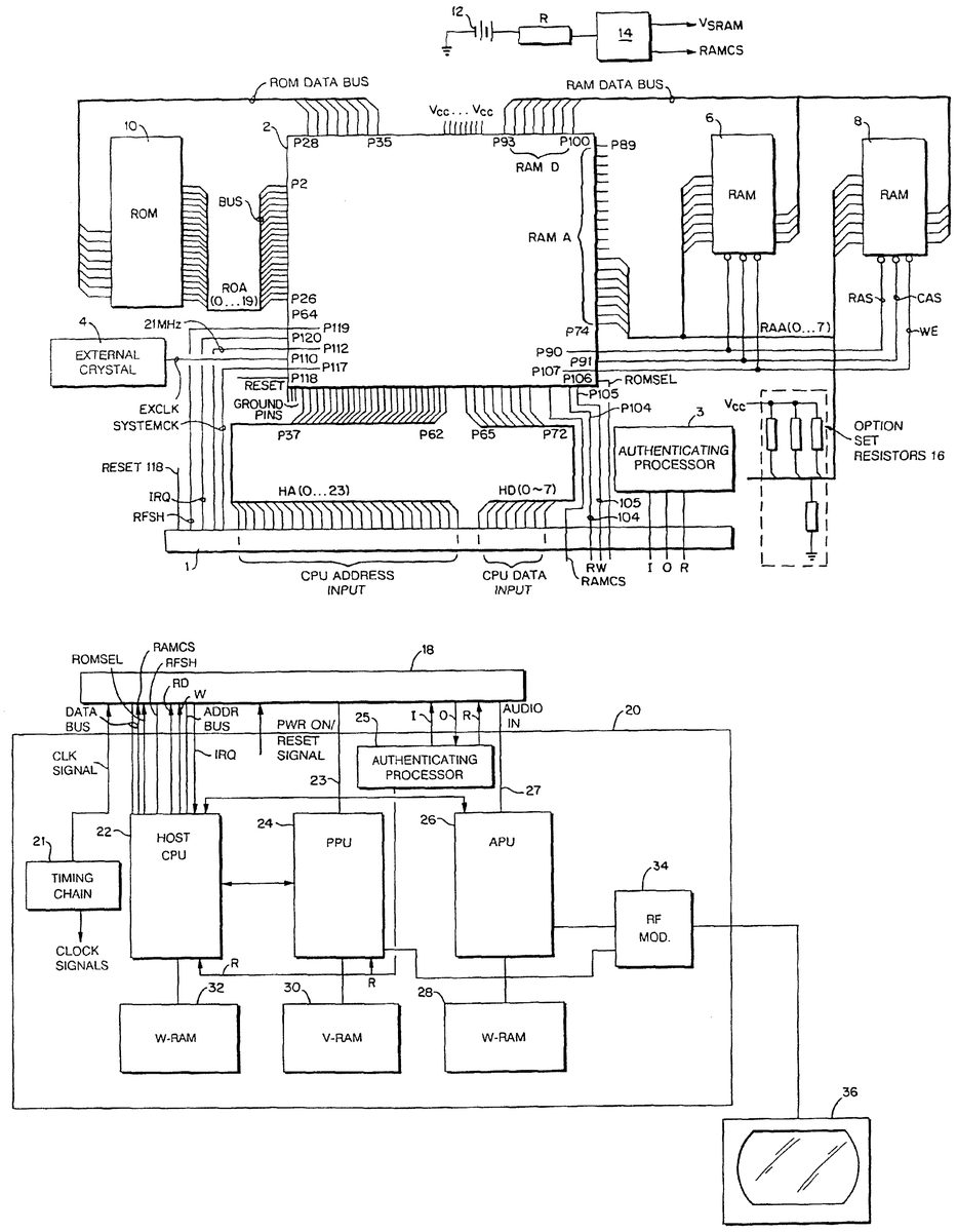
FIG. 1shows an exemplary video game cartridge/external memory system in accordance with an exemplary embodiment of the present invention. The game cartridge includes a printed circuit board (not shown) on which all of theFIG. 1components are mounted. The cartridge includes an array of connector electrodes1disposed at an insertion end of the printed circuit board for transmitting signals to and from the Super NES main control deck. The array of connector electrodes1is received by a mating connector disposed in the Super NES main control deck.
In accordance with the present exemplary embodiment, the Mario chip (graphics coprocessor)2embodied on the game cartridge is a 100 to 128 pin integrated circuit chip. The Mario chip receives many control, address and data signals from the host processing system (e.g., the Super NES). For example, the Mario chip2receives a 21 MHz clock input from the host processing system via pin P112, and a system clock input which may be 21 MHz (or another predetermined frequency) via pin P117. The system clock input may be used, for example, to provide the Mario processor with memory timing information for host CPU memory accesses and to provide clock signals for timing operations within the Mario chip. The Mario chip2also includes an optional, external clock input (pin P110) which couples the Mario chip to an external crystal4, to drive the Mario CPU, for example, at a higher frequency clocking rate than the 21 MHz received from the host system.
Host CPU address inputs (EA) are coupled to the Mario chip2via pins P37to pins P62from the host processing system (e.g., Super NES CPU/Picture Processing Unit PPU) address bus. Similarly, data inputs (HD) from the host system are coupled to the Mario chip2via pins P65-P72from the host CPU data bus. The Mario chip2additionally receives from the host CPU a memory refresh signal RFSH via P119, a reset signal via pin P118read and write control signals via pins P104, P105. The Mario chip generates an interrupt request signal IRQ and couples the signal IRQ to the Super NES via pin P120. Other control signals are received from the Super NES such as a ROMSEL signal via pin P106which may, for example, initiate a host program ROM10access. Additionally, the cartridge includes an authentication processor3which exchanges data with a Super NES authenticating processor on input I, output O, and reset R lines. The authenticating processor3and the security system used to authenticate game cartridges may be of the type shown in U.S. Pat. No. 4,799,635, which patent is incorporated herein by reference.
The Mario chip is coupled to RAMs6and8via the RAM address bus (RAM A), and RAM address pins P74-P91and the RAM data bus (RAM D) and data pins P93-P100. These RAMs may be dynamic memory devices controlled in part using row address and column address strobe signals (RAS, CAS) coupled via pins P90and P91, respectively. One or more static RAMs may be utilized instead of dynamic RAMs and pins P90and P91would then be used to couple address signals to their respective RAMs without the row address and column address strobe signals. A write enable control signals WE is appropriately coupled to RAM6and8via pin P107.
The read and write control signals (R, W) are generated by the host CPU and coupled to the Mario chip via pins P104and P105. By monitoring these read and write lines, the Mario chip can determine the nature of the memory access operation the Super NES CPU is attempting to perform. Similarly, virtually all address and control lines from the host system are monitored by the Mario chip to keep track of what the host CPU is attempting to do. The ROM and RAM addressing signals received by the Mario chip are monitored and passed on to the appropriate memory device. In this regard, the ROM addresses are coupled to program ROM10via the ROM address bus and pin P2to P26and the RAM address is coupled to RAMs6and8via pins P74to pins P91. The ROM and RAM data inputs from the host CPU are appropriately coupled to ROM10via the ROM data bus and pins P28-P35and via pins P93to P100, respectively.
It should be recognized that the Mario chip may be utilized in conjunction with a wide range of different memory devices in addition to the ROM and RAM's described herein. For example, it is contemplated that the Mario chip may be advantageously utilized in conjunction with video game systems using CD ROM's.
For example, inFIG. 1, instead of using ROM10, a CD ROM (not shown) may be used to store character data, program instructions, video, graphic, and sound data. A conventional-type CD player (also not shown) suitably connected to the Mario chip2to receive memory address signals over address bus P2-P26for accessing data and/or instructions over data bus P28-P35. The specific structural and operational details of CD players and CD ROM storage systems are well known to those skilled in the art. One advantage provided by CD ROM storage is a significant reduction in the cost of storage per byte of information. Data may be stored at a cost between 100 to 1000 percent less than storage on semiconductor ROM. Unfortunately, the memory access/read time for CD ROM is even slower than that for semiconductor ROM.
The Mario chip uses a three bus architecture which permits information on at least three buses to be utilized in parallel. In this regard, in the game cartridge shown inFIG. 1, the Mario chip2is coupled to a ROM bus (including ROM data lines, ROM address lines and control lines), a RAM bus (including RAM address lines, data lines, and control lines) and a host processor bus (including host address, data and control lines).
The Mario chip architecture permits pipelined operations to occur to optimize throughput. In this regard, the Mario chip can be reading a data byte from ROM, while processing other data, while writing yet further data to RAM to permit 3-D related graphics to be performed very efficiently. As is described further below, the Mario chip2uses a 16-bit architecture internally and yet is designed to interface with 8-bit ROM10and RAM6,8chips. Internally, all internal data buses and internal registers are 16-bits. Reads from ROM10and writes to RAM6,8are “buffered” and typically do not slow down program execution.
Similarly, the Mario chip2may access instructions and graphics data from CD ROM and write that information into RAM6,8for subsequent DMA transfer into the video RAM of the host processor, e.g., Super NES picture processing unit (PPU). Those skilled in the art will appreciate that the Mario chip2may be programmed to coordinate transfer of data from the CD ROM directly to the video RAM of the PPU, bypassing the RAM storage and access operations.
The extremely fast processing speed of the Mario chip2makes CD ROM storage practical for graphics applications despite the long read access time of CD ROMs. Video and audio data are compressed using conventional data compression techniques before storage on CD ROM. Data compression and decompression techniques are well known to those skilled in the art. After accessing compressed data from the CD ROM, the Mario chip2decompresses the data using conventional data decompression algorithms in much shorter time periods than can be achieved by conventional graphics processors. Because it operates with a 21 MHz clock, the Mario chip2completes decompression within prescribed time periods for data transfer to RAM6,8.
Thus, large amounts of video and audio data are accessed (in compressed form) in typical CD ROM access time periods. However, the effect of those relatively long access times is minimized because after data decompression by the Mario chip2, the actual access time per data byte is significantly reduced. With the Mario chip2performing decompression, the host graphics processor, e.g. the Super NES PPU, is free to perform other processing tasks. Of course, if speed is not an issue for a particular application, the Mario chip2can access data from CD ROM in uncompressed form.
The cartridge may also include a battery backup when static RAM is used. A backup battery12is coupled to a conventional backup battery circuit14via a resistor R to provide a backup voltage (RSRAM) for static RAM and a static RAM chip select signal RAMCS in case of loss of power to provide a data saving feature.
Additionally, coupled to the RAM address bus, are option setting resistors16. In normal operation, the Mario chip address lines are output to RAMs6and8. However, during reset or power-on operations, these address lines are used as input lines to generate either a high or low signal depending upon whether they are tied to a predetermined voltage VCC or ground. In this fashion, a “1” or “0” is appropriately read into an internal Mario chip register. After reset, depending upon the setting of these resistors, the Mario chip can determine (during program execution), for example, the multiplier clocking rate, the RAM access time to which the Mario chip is coupled, the clocking rate to be used with other operations within the Mario chip, etc. Through the use of these option setting registers, the Mario chip is, for example, adaptable to be used with a number of different types of memory devices without requiring any Mario chip design modifications. For example, if a dynamic RAM setting is detected then refresh signals will be applied at appropriate times. Additionally, the option settings may be used to control the speed at which, for example, the processor multiplier circuits operate and to permit other instructions to be executed by the graphics processor at a faster rate than it is possible to execute certain multiply instructions. Thus by initiating a delayed multiply execution, the remaining instructions can run at a faster clock rate than the rate otherwise possible (e.g., the processor may, for example, be clocked at 30 megahertz, whereas the option settings would effectively cause the multiply instructions to be executed at 15 megahertz).
FIG. 2is block diagram of an exemplary host video game system to which the exemplary game cartridge set forth inFIG. 1is designed to be coupled.FIG. 2may, for example, represent the Super NES currently sold by Nintendo of America. The present invention, however, is not limited to Super NES related applications or systems having a block diagram such as that shown in FIG.2.
The Super NES includes within its control deck20, a 16-bit host CPU which may, for example, be a 65816 compatible microprocessor. The CPU22is coupled to a working RAM32, which may, for example, include 128 K bytes of storage. The CPU22is coupled to a picture processing unit (PPU)24which in turn is coupled to a video RAM30which may, for example, include 32K words of storage. The CPU22has access to the video RAM30via the PPU24during vertical or horizontal blanking intervals. Thus, the CPU22can only access the video RAM30through the PPU24at times other than during active line scan when the PPU24is accessing video RAM. PPU24generates a video display on a user's television36from video RAM30. CPU is also coupled to an audio processing unit APU26which is coupled to a working RAM28. The APU26which may comprise a commercially available sound chip generates the sounds associated with the video game program stored on the game cartridge in ROM10. The CPU22can only access the working RAM28via APU216. The PPU24and APU26are coupled to the user's home television36via RE modulator unit34.
The video RAM30in the Super NES must be loaded with appropriate character data stored in the program ROM10in the cartridge (which stores not only the game program, but also the character data used during game play). Any moving object, e.g., sprite information, or background information to be displayed must be resident in video RAM30before use. The program ROM10is accessed by the CPU22host address and data buses via a mating connector18which is coupled to the printed circuit board edge connector1shown in FIG.1. The PPU24is connected to the game cartridge via shared host CPU data and address buses and connector23so as to provide a path for PPU data and control signals to be coupled to the cartridge. The APU26is connected to the game cartridge via shared host CPU buses and audio bus27.
The CPU22address space is mapped such that program ROM10locations begin at location0and is typically divided into 32 K byte segments. The program ROM uses approximately one-half of the CPU address space. The top locations in each CPU address space 32 K byte segment is typically utilized to address working RAM32and various registers. The program ROM10typically is four megabytes. The CPU22used in the Super NES is capable of addressing the entirety of the program ROM10. On the other hand, the Mario chip2only includes a 16 bit program counter and thus includes bank registers for selecting between the 32 K byte banks in the program ROM10.
In the present exemplary embodiment, the Mario chip has a full 24 bit address space that corresponds with the Super NES memory map. This contains the ROM10at the position starting at location $00:8000, and the RAM chip6,8on the cartridge starts at location $70:0000.
Since the ROM10and RAM6,8on the cartridge are on separate buses they can be accessed in parallel by the Mario Chip. Also RAMs6,8can be accessed at a faster rate than ROM and the Mario chip is designed to utilize this performance advantage. The Mario chip has no access to any memory that is inside the Super NES, i.e., no access to the working RAM32or PPU video RAM30.
In order for the Mario chip to process data, or draw into a bitmap, data must be contained within the Mario cartridge RAM chip6,8. Thus, any variables which are shared between the NES CPU program and the Mario chip program must be within the Mario cartridge RAM chip6,8. Any prestored data that the Mario chip program needs to use can be in ROM10and any variables will be in RAM6, B.
Any private variables only required by the Super NES program do not need to be in cartridge RAM6,8. In fact, since this RAM6,8is at a premium in terms of memory space, it is advisable to allocate cartridge RAM6,8on a high priority requirement basis. Any non-essential variables should be stored in Super NES internal RAM32.
The bitmap that the Mario Chip writes into is in Mario cartridge RAM6,8and will be DMA transferred under control of the Super NES into the PPU's video RAM30when each bitmap frame has been fully rendered.
The Super NES's CPU22has access to all internal RAM within the Super NES control deck just as if the Mario chip were not present. The Mario chip has no access to this RAM so all data transferred between the Mario ROM/RAM chips and internal Super NES RAM must be initiated by the CPU22itself. Data can be transferred via CPU22programming, or block moved via DMA transfer. The Mario cartridge ROM10and RAM6,8are mapped in as usual on all game programs.
The CPU22has control over which CPU has temporary access to the cartridge ROM or RAM chips. On power up or reset conditions, the Mario chip is turned off and the CPU22has total access to the cartridge ROM and RAM chips. In order for the Mario chip to run a program, it is necessary for the CPU22program to give up its access to either the ROM or RAM chip, preferably both, and either wait for the Mario chip to finish its given task, or alternatively the CPU22can copy some code into internal work-RAM32and execute it there.
The Mario chip has a number of registers that are programmable and readable from the Super NES CPU side. These are mapped into the CPU22memory map starting at location $00:3000.
As indicated inFIG. 2, the Super NES generates and receives a variety of control signals. When the Super NES CPU22needs to access program ROM10, it generates a control signal ROMSEL. To initiate a memory refresh, the Super NES generates a refresh signal RFSH. When the Mario chip completes an operation, it transmits an interrupt signal IRQ on an interrupt request line associated with the Super NES CPU. The CPU22additionally generates read and write signals.
System timing signals are generated from timing chain circuitry21within the control deck20. A power-on/reset signal is also generated within the main control deck20and coupled to the game cartridge.
The Super NES also includes an authenticating processing device25which exchanges data on input I output O, and reset R conductors with an authenticating processing device3on the game cartridge in accordance with the above identified U.S. Pat. No. 4,799,635. The processing device25as taught by U.S. Pat. No. 4,799,635 holds the CPU22in a reset state until authentication is established.
The Super NES video game machine which is represented in block form inFIG. 2has only been generally described herein. Further details regarding the Super NES including PPU24may, for example, be found in U.S. application Ser. No. 07/651,265, now U.S. Pat. No. 5,327,158, entitled “Video Processing Apparatus which was filed on Apr. 10, 1991, which application has been expressly incorporated herein by reference. Still further details such as how information is transferred between the Super NES and the game cartridge may be found in U.S. application Ser. No. 07/749,530, now U.S. Pat. No. 5,291,189, filed on Aug. 26, 1991, entitled “Direct Memory Access Apparatus in Image Processing System and External Storage Device Used Therein” and in U.S. application Ser. No. 07/793,735, filed Nov. 19, 1991, entitled, “Mosaic Picture Display Apparatus and External Storage Unit Used Therefor”, which applications are incorporated herein by reference.
In some applications, the inventors have recognized that more information may need to be transferred during vertical blanking using such host processor DMA circuits than is actually possible. Accordingly, it may be desirable to extend vertical blanking time—even if it results in slightly shrinking the picture size. By using this approach, significant advantages are realized in terms of processing speed and picture update rate.
FIG. 3shows a perspective view of an exemplary mechanical design for a game cartridge case19for housing the Mario chip and other cartridge structure shown in FIG.1. Similarly,FIG. 3shows the perspective view of an exemplary exterior housing for a video game control deck20for housing the Super NES video game hardware shown in FIG.2. The mechanical design for such video game control deck20and associated removable game cartridge19is shown in FIGS. 2-9 of U.S. application Ser. No. 07/748,938, now U.S. Pat. No. 5,192,082, filed on Aug. 23, 1991, entitled, “TV Game Machine”, which application is hereby incorporated herein by reference.
FIGS. 4A and 4Bare a block diagram of the Mario chip2shown in FIG.1. Focusing first on the various buses shown inFIGS. 4A and 4B, the instruction bus INSTR is an 8-bit bus that couples instruction codes to various Mario chip components. The X, Y and Z buses are 16-bit data buses. The HA bus is a 24-bit host system address bus that, in the presently preferred embodiment is coupled, in use, to the Super NES address bus. The HD bus is an 8-bit host data bus which is coupled, in use, to the Super NES data bus. The PC bus is a 16-bit bus which couples the output of the Mario chip program counter (i.e., register R15in general register block76) to various system components. The ROM A bus is a 20-bit ROM address bus. The ROM D bus is an 8-bit ROM data bus. The RAM A bus is a bit RAM address bus. The RAMD_IN bus is an 8-bit RAM read data bus, and RAMD_OUT is an 8-bit RAM write data bus.
The Mario chip and the Super NES share the cartridge RAM6,8which serves a's the main mechanism for passing data between the Mario chip and the Super NES. The Super NES accesses the Mario chip via the address and data buses HA and HD. The Mario chip registers76are accessed by the Super NES via the Super NES address bus HA.
The Super NES accesses the cartridge program ROM10and RAM6,8via the Mario chip2. The ROM controller104and the RAM controller88receive memory access related signals generated by the Super NES to respectively initiate ROM and RAM memory accesses. By way of example, a RAM select signal RAMCS is used by the Mario chip2to confirm that the Super NES is attempting to address the RAM.
The X, Y and Z buses shown inFIGS. 4A and 4Bare the internal Mario chip data buses. The X and Y buses are source data buses and the Z data bus is a destination bus. These buses carry 16 bits of parallel data.
While executing instructions, the Mario chip2may place the source of data for an instruction on the X and/or Y buses and the destination data on the Z bus. For example, in executing an instruction which adds the contents of two registers and places the results in a third register, arithmetic and logic unit (ALU)50receives the contents of two source registers via the X and Y bus couples the result to the Z bus (which in turn is coupled to a specified register in block76). Control signals resulting from the decoding of an instruction operation code by the instruction decoding circuitry60in the Mario chip2are coupled to the ALU50to initiate an ADD operation.
As noted with respect to the description ofFIG. 1, the Mario chip is coupled to a ROM bus, a RAM bus and a Super NES host bus which are capable of communicating signals in parallel. The Mario chip2monitors the control, address and data signals transmitted via the host Super NES bus to determine the operations which the host system is performing. The cartridge ROM bus and the cartridge RAM bus may be accessed in parallel depending upon the Super NES operation being performed at any given time. In conventional Super NES game cartridges, the host CPU address and data lines are coupled directly to the RAM and ROM, such that the RAM and ROM may not be accessed in parallel.
In accordance with one aspect of the present invention, the Mario chip2physically separates the ROM bus and the RAM bus as shown inFIG. 1from the Super NES buses. The Mario chip2monitors the signals transmitted on the Super NES buses and determines what signals need to be coupled to the ROM chip and the RAM chip via two separate ROM and RAM buses which are not time shared. By separating the ROM and RAM buses, the Mario chip2is able to read from ROM and write to RAM simultaneously. In this fashion, the Mario chip can efficiently operate with inexpensive ROM chips which have access times which are significantly slower than RAM access times without having to wait for the ROM accesses to be completed before accessing RAM.
Turning toFIG. 4A, as noted above, the Mario chip2is a fully programmable processor, and includes an ALU50. The ALU50executes all the arithmetic functions embodied within the Mario chip except for multiply operations which are handled by multiplier64and certain pixel plotting operations handled by plot hardware52. Upon receipt of an appropriate control signal from instruction decoder60, the ALU50performs addition, subtraction, EXCLUSIVE-OR, shift and other operations. As shown inFIG. 4A, ALU50receives information to be operated on from the X, Y buses, performs the operation initiated by a control signal received from instruction decoder60, and couples the results of the operation to the Z bus. The ALU is described in further detail below in conjunction with FIG.6.
The Mario chip2additionally includes special purpose hardware to enable 3-D type special effects and other graphic operations to be efficiently performed so that video games utilizing these features may be practically realized. In this regard, the Mario chip2includes plot hardware52which assists in converting in real time from pixel coordinate addressing to character map addressing of the nature utilized in the Super NES.
Advantageously, the Mario chip may be programmed by specifying X and Y coordinates which define the location of each pixel on the display screen.
Thus, graphic operations are performed based on a programmer specifying pixels and the plot hardware circuit52on the fly converts pixel specifications into properly formatted character data. The character data is then mapped into the desired place for display in the Super NES video RAM30shown in FIG.2. In this fashion, the Mario chip programmer need only consider the Super NES video RAM30as a bit map when in reality, it is a character map.
The plot hardware52responds to various plotting related instructions to permit programmable selection of an X and Y coordinate on the display screen and a predetermined color for a particular pixel and to plot corresponding pixels such that the X and Y coordinate is converted into an address which corresponds to a character definition of the form which is used to drive the Super NES video RAM30.
The plot hardware52has associated data latches which permit buffering of as much pixel data as possible prior to writing to cartridge RAM to minimize RAM data transactions. After the X and Y coordinate data is converted and buffered in the plot hardware52, character definition data is then transferred to the cartridge RAM.
The plot hardware52receives X, Y coordinate data via a PLOT X register56and PLOT Y register58, respectively. In the presently preferred embodiment, the PLOT X and PLOT Y registers are not separate registers (as shown inFIG. 4A) but rather are Mario chip general registers (e.g., registers R1and R2registers in register block76shown in FIG.4B).
The plot hardware52also receives pixel color information via a color register54. As will be described further below, the color of each pixel that is displayed is stored in an 8×8 register matrix, with each pixel color specification, occupying a column of the matrix.
The plot hardware52processes and couples the character address and data associated with the X, Y and color input to the character RAN6,8. The character address is forwarded via output lines53to the RAM controller88and to a RAM address bus RAN A. The character data is coupled to the character RAM via output line55, multiplexer93and RAN data bus RAMD_OUT. The plot hardware52permits pixels within a character to be addressed individually, to thereby provide the programmer a “virtual” bit map display system, while maintaining compatibility with the Super NES character format. The “virtual” bit map is held in the cartridge RAN and is transferred to the Super NES video RAN30on the completion of the display of each frame using, for example, the DMA circuitry in the above-identified application Ser. No. 07/749,530, now U.S. Pat. No. 5,291,189. The plot hardware52permits high speed individual pixel control so that certain 3-D graphics effects involving rotating and scaling objects become practically realizable.
Because of the conversion from pixel to character format, the plot hardware52also receives information relating to other pixels in the vicinity of the current pixel X, Y from a cartridge RAM6,8via RAMD_in data latch82and input line83. By using previous pixel data retrieved from RAM6,8and temporarily stored in the RAM data latches, the number of writes to RAM may be minimized. The RAM data latches80,84, and86shown inFIG. 4Aalso serve to buffer color data received regarding a pixel which has been stored in multiple bit planes in cartridge RAM to provide plot hardware52with such data.
RAM data latch80is coupled to the Super NES data bus so that the Super NES can read the contents of the data latch. RAM data latches80,82,84, and86are controlled by the RAM controller88. RAM data latches84and86operate to receive data from RAM6,8and couple data from RAM6,8to the destination Z bus for loading into a predetermined register in register block76. Additionally coupled to RAM controller88is a latch90which buffers RAM addresses. The address stored in latch90is utilized by RAM controller88for addressing RAM6,8via the RAM A bus. RAM controller88may also be accessed by the Super NES via address bus HA.
The plot hardware52also responds to a READ PIXEL instruction which reads the pixel color information for a horizontal position defined by the contents of register R1and the vertical position defined by the contents of register R2and stores the result in a predetermined register in the register block76via the destination Z bus and output line87. The PLOT hardware52is described in further detail in conjunction with the description ofFIGS. 7,8A, and8B.
Pipeline buffer register62and an ALU controller instruction decoder60are coupled to instruction bus INSTR and operate to generate the control signals CTL (utilized throughout the Mario chip) to initiate operations in response to commands placed on the instruction bus. The Mario chip2is a pipelined microprocessor which fetches the next instruction to be executed while it is executing the current instruction. Pipeline register62stores the next instruction(s) to be executed so as to permit execution of instructions in one cycle, if possible. The instructions which are placed on the instruction bus are addressed by the contents of the program counter stored in a register, which may, for example, be register R15in register block76shown in FIG.4B.
The instructions executed by the Mario chip2may either be obtained from program ROM10as shown inFIG. 1or the Mario chip's internal cache RAM94or from the cartridge RAM6,8. If the program is being executed out of ROM10, the ROM controller104(shown inFIG. 4B) will fetch the instruction and place it on the Mario chip instruction bus INSTR. If a program instruction is stored in the cache RAM94, then the instruction will be placed on the instruction bus directly from cache RAM94via cache RAM output bus95.
The host CPU, i.e., the Super NES, is programmed to allocate portions of the program ROM10for Mario chip program instructions. The super NES program commands the Mario chip to perform a predetermined function and then provides the Mario chip with the address in ROM10for accessing the Mario chip program code. Pipeline register62fetches instructions one byte ahead of the instruction being executed to provide the instruction decoder60with instruction related information for the decoder to be able to anticipate what is about to occur during program execution to permit look ahead related processing. The decoding and control circuitry in block60generates control signals for commanding the ALU50, plot hardware52, cache control68, etc., to perform the operation indicated by the instruction code being executed.
The Mario chip also includes a high speed, parallel multiplier64that is separate from ALU50. The multiplier64in response to predetermined instructions operates to multiply two B-bit numbers received from the X and Y source buses and load the 16-bit result onto the destination Z bus. This multiply operation is performed in one cycle if possible. Either number input to the multiplier64may be signed or unsigned. Multiplier64also is capable of performing long multiply operations, whereby two 16-bit numbers are multiplied to generate a 32-bit result. The multiplier64also includes associated partial product registers66to store partial products generated during the multiplication operation. The multiplier64is enabled by a control signal from the instruction decoder60when a multiply operation code is decoded. The multiplier64will execute long multiply instructions involving the multiplication of 16-bit words in a minimum of four clock cycles.
The long multiply instruction has a format:
R4(low word), DREG (high word)=Sreg*R6. This instruction is executed to multiply the source register by the contents of register R6and store a 32-bit result in registers R4/DREG (low/high). The multiply is signed and sets zero and sign flags on the 32-bit result.
The operation takes place in accordance with the following six steps:Step 1: Unsigned multiply R4[0 . . . 15]=SREG [0 . . . 7]*R6[0 . . . 7]Step 2: X signed. R4[0 . . . 15]=R4[0 . . . 15]+256*SREG [8 . . . 15]*R6[0 . . . 7]. Top eight bits of the product are ignored, but carry from addition preserved.Step 3: X signed. R5[0 . . . 15]=CY+(R6[8 . . . 15]*SREG [0-7])÷256; sign extended.Step 4: X unsigned, Y signed. R4[0 . . . 15]=R4[0 . . . 15]+256*SREG [0 . . . 7]*R6[8 . . . 15]. The top eight bits of the product are ignored, but carry from the addition is preserved.Step 5: Y signed. R5[0 . . . 15]=R5[0 . . . 15]+CY+SREG [0 . . . 7]*R6[8 . . . 15])÷256; sign extended.Step 6: X, Y signed. R5[0 . . . 15]=R5[0 . . . 15]+RY [8 . . . 15]*R6[8 . . . 15].
The multiplier64utilized in the present exemplary embodiment may be, for example, of the type described inDigital Computer Arithmetic, by Cavanaugh, published by McGraw-Hill, 1984.
Turning toFIG. 4B, cache controller68(which is shown in further detail inFIG. 14) permits a programmer to efficiently initiate loading into cache RAM94the portion of the program desired to be executed at high speed. Such “caching” is typically utilized in executing small program loops which occur frequently in graphics processing. The Mario chip instruction set includes a “CACHE” instruction. Any instructions immediately following the CACHE instruction is loaded into the cache RAM until the cache RAM is full. When the CACHE instruction is executed, the current program counter state is loaded into the cache base register70. Thus, the contents of the cache base register70defines the starting location at which caching has been initiated.
Most instructions execute in one cycle. Instructions coming from relatively slow external memories like ROM10or RAM6,8must be fetched before they are executed. This will take an extra 6 or so cycles. To enhance program execution speed, the ‘cache’ RAM94that is inside the Mario chip itself should be used.
Cache RAM94may be a 512-byte instruction cache. This is a relatively small size compared to the size of the average program, so the programmer must decide how best to utilize the cache memory94. Any program loop that can fit into the 512 bytes cache size can run at full speed, one cycle for both fetch and execute. Because of the split busses, both ROM and RAM can be simultaneously accessed while executing code from internal cache94.
The cache RAM94may be advantageously used to rotate a sprite by running a loop inside the cache94that would read the color of each pixel from ROM10while it is performing the rotation and scaling calculations, while it is using the PLOT instruction (to be described below) to write the pixel to RAM6,8. All that happens in parallel, giving very fast throughput slowed down by the slowest operation. The slowest operation is usually ROM data fetching, which is why the Mario chip is designed to use buffered access to ROM and RAM.
When compared with running from the relatively slow ROM10, a program will run about 6 times faster from inside the cache RAM94, but first it has to be loaded from ROM into the cache94. This is done by placing an instruction at the start of any loop to be cached. Only the first 512 bytes of the loop will be cached, taken from the address of the CACHE instruction. While executing the code for the first iteration of the loop, the program will be coming from ROM10and copied into cache RAM in 16-byte chunks. All further iterations of the loop will come from the cache RAM94instead of ROM10.
CACHE instructions can be used liberally in front of any repetitive program loops. Only subsequent iterations of a loop will benefit from being in cache. If a program loop is bigger than 512 bytes and overflows the cache94, it will still work correctly, but only the first 512 bytes will run from cache94and the remainder will run from ROM10as usual. This gives a partial speed boost, but is not ideal.
A cache tag bit register72which, in the preferred embodiment, is part of the cache controller68identifies the memory locations which have been loaded in the cache RAM94. The cache tag bits permit the Mario chip to quickly determine whether a program instruction is executable from the faster cache RAM rather than from the program ROM10. The cache RAM94may be accessed by the cache controller68or the Super NES via the Super NES address bus HA via multiplexer96.
The cache controller68is coupled to the program counter bus PC to load the cache base register70and perform cache memory address out-of-range checking operations.
Similar to the parallelism achievable in reading from ROM10, the Mario chip also provides a way of writing to RAM6,8in parallel. Whenever a Mario register is written to RAM6,8, it will initiate a separate RAM write circuit, e.g., in RAM controller88, to do the memory transaction. This will take typically 6 cycles, but it will not delay the processor while it is doing so, provided the programmer avoids doing another RAM transaction for that time. For instance, it is faster to interleave other processing in between each store instruction. That way the RAM write circuit has time to do its job. If two writes are used in a row, the second one would delay the processor while the first one is being written.
For example (using instructions from the instruction set to be described below):
FROMR8; Store R8 into (R13)SM(R13)SM(R14); Store R0 into (R14)TOR1FROMR2ADDR3; Performs:r1=r2+r3TOR4FROMR5ADDR6; Performs:r4=r5+r6
Notice that the two store instructions are too close to each other. The second one will take 6 cycles longer because the RAM bus is busy trying to complete the first store instruction.
A better way of writing the code that will run faster would be to space out the two store instructions with other useful code. For example:
FROMR8; Store R8 into (R13)SM(R13)TOR1FROMR2ADDR3; Performs:r1=r2+r3TOR4FROMR5ADDR6; Performs:r4=r5+r6SM(R14); Store R0 into (R14)
In this fashion, a few more instructions may be executed in parallel at the same time that the first store instruction results in the writing to RAM. Then the second store operation can be done a few cycles later.
The instruction set described below includes a fast instruction for writing back a register to the last used RAM address. This allows for “bulk” processing of data, by loading the value from RAM, doing some processing on it, then storing it back again fast.
Turning back toFIG. 4B, an immediate data latch74is coupled to the instruction bus. This data latch74permits the instruction itself to provide the source of data so that no source register need be specified by an instruction. The output of the immediate data latch74is coupled to the destination Z bus, which in turn is coupled to a predetermined one of the registers in register block76. The instruction decoding circuit60decodes an “immediate” data instruction and initiates the performance of the appropriate transfer to register operation.
The GET B register98shown inFIG. 4Bis used in conjunction with the delayed/buffered read operation described above. In this regard, given the widespread use of relatively slow access time ROMs, prior art processors have typically had to wait until a data fetch is completed, whenever executing a ROM. By utilizing the delayed/buffered fetch mechanism described below, other operations may be performed while the data fetch is accomplished. In accordance with this mechanism, if register R14in register block76is accessed or modified in any way, ROM or RAM fetches are initiated automatically at the address identified by the contents of R14.
As indicated inFIG. 4B, the register R14is coupled to ROM controller104. Any time the contents of register R14is modified in any way, ROM controller104operates to initiate a ROM access. The results of accessing the ROM are loaded into the GET B register98via multiplexer102which is coupled to the ROM data bus ROMD. Instructions identified below permit accessing the information buffered in the GET B register98. This information is loaded onto the destination Z bus via multiplexer100and then into one of the registers in register block76.
In this fashion, if a data fetch from ROM is known to take a predetermined number of processing cycles, that fetch can be initiated and instead of waiting without performing other operations, the Mario chip can execute, for example, unrelated code after such data fetch has been initiated. The GET B register98may also be utilized to store information retrieved from RAM6,8via multiplexer102as shown in FIG.4B.
Embodied within register block76are sixteen 16-bit registers (R0-R15). Registers R0-R13are general purpose registers (although some of these registers are often used for special purposes to be described below). As described above, register R14is used as a pointer for reading memory, and, when modified, a read cycle from ROM (or RAM) is initiated. The byte read is stored in a temporary buffer (GET B register98) for later access by a GET L or GET H command. Register R15is the program counter. At the start of each instruction it points to the next instruction being fetched.
Register R0is a general purpose register, which typically operates as an accumulator. It is also the default source and destination register for most single cycle instructions. If, for example, the contents of R0and R4are desired to be added together it is only necessary to expressly specify register R4.
Registers R11, R12and R13are specially utilized when a loop instruction is executed. Register R13stores an address of the instruction to be executed at the top of the loop, and register R12stores the number of times the loop is to be executed. If the contents of register R12is non-zero, then the instruction at the address specified by the contents of R13is loaded into the program counter (R15) and executed. Register R11stores the address to be returned to after the loop is completed.
Register control logic78is coupled to register block76and controls access to general registers R0to R15. Depending upon the format of the particular instruction being executed, instruction decode logic60will specify one or more registers R0-R15. Register control logic78specifies which register the next instruction to be executed will need to utilize. The register control logic78couples the outputs of the appropriate register to the X and Y bus. Additionally, as indicated byFIG. 4B, the appropriate register R0-R15receives the information from the Z bus under the control of register control78.
ROM controller104upon receipt of an address from either the Super NES address bus HA or the Mario chip will access that address. ROM controller104is shown in further detail in FIG.13. Accessed information from ROM10may be loaded into the cache RAM94for fast instruction execution. The ROM and RAM controllers104,108both have bus arbitration units which arbitrate between Super NES and the Mario chip access attempts.
As will be described further below, the Mario chip also utilizes status registers (e.g., within register block76or in RAM6,8) which are accessible by the Super NES CPU and which store flags for identifying status conditions such as 0 flag, carry flag, sign flag, overflow flag, “GO” flag (where 1 indicates that the Mario chip is running and 0 indicates that the Mario chip is stopped); a ROM byte fetch-in-progress flag (indicating that register R14has been accessed); various mode indicating flags including an ALT1flag, ALT2flag, immediate byte-low and immediate byte-high flags, and flags indicating that both a source and destination register has been set by a “WITH” prefix command, and an interrupt flag.
The Mario chip represented in block diagram form inFIGS. 4A and 4Bis utilized by the Super NES which turns the Mario chip on and off to perform tasks many times a second. Initially, when the Super NES is turned on, the game program stored in ROM10is booted up. It is noted that prior to execution of the game program by the Super NES and Mario chip processors, the game cartridge is first authenticated. By way of example only, such authentication may take place by initially placing the Super NES CPU in a reset state and executing authenticating programs in authenticating processors associated with the game cartridge and the Super NES main control deck in accordance with the teachings in U.S. Pat. No. 4,799,635.
The Mario chip is initially in a switched-off state. At this point in time, the Super NES has unrestricted access to the game cartridge program ROM and the game cartridge RAM. When the Super NES has need to use the Mario chip processing power to perform either graphics operations or mathematical calculations, the Super NES stores the appropriate data it desires the Mario chip to process in the cartridge RAM (or in predetermined Mario registers) and loads the Mario chip program counter with the address of the Mario program to be executed. The data to be processed by the Mario chip may be predetermined X, Y coordinate data of objects which must be rotated and enlarged or reduced. The Mario chip can execute programs which implement algorithms to manipulate the background and foreground of sprites or moving objects of varying number. The use of the Mario chip speed enhancing hardware and software results in high speed performance of such operations.
The use of the Mario chip to process sprites can expand the capabilities of the overall video game system considerably. For example, the Super NES is limited to displaying126sprites per frame. With the use of the Super Mario chip virtually hundreds of sprites may be displayed and, for example, rotated.
When the Mario chip has completed the function requested by the Super NES, a STOP instruction is executed, and an interrupt signal is generated and transmitted to the Super NES to indicate that the Mario chip has completed its operation—which, in turn, indicates that it is ready to perform the next task.
The Mario chip may be utilized to do small tasks such as a high-speed multiplication task or may be utilized to draw a screen full of sprites. In either event, the Super NES is free to do processing in parallel with the Mario chip provided the Super NES stays off the RAM or ROM buses when such buses are being used by the Mario chip. It is noted that if the Super NES gives the Mario chip control of both the RAM and ROM buses on a game cartridge, the Super NES may, nevertheless, be able to execute programs out of its working RAM32shown in FIG.2. Thus, the throughput of the entire system may be increased by copying a Super NES program to be executed from program ROM to its working RAM; while, at the same time, executing a program by the Mario chip.
A flowchart is shown inFIG. 5which represents the sequence of operations performed by a “RUN MARIO” program executed by the host CPU (e.g., the Super NES CPU) for starting the Mario chip to fetch and execute code from ROM at the required address. The routine represented byFIG. 5will be typically executed by the Super NES CPU after copying the routine from the program ROM10to its working RAM32shown in FIG.2. This routine is executed by the host CPU any time the Mario chip is required to perform an operation.
As indicated in block125when the RUN MARIO host CPU routine is executed, initialization operations are performed including preserving the Super NES registers. During the initialization step, this routine is copied from program ROM10to the host CPU's working RAM32.
As indicated at block127, the ROM10code bank storing the Mario program code to be executed is loaded in a Mario chip register. Additionally, the actual address within the code bank is stored in a Mario chip screen base register as indicated at block129.
Thereafter, as indicated in block131, I/O input/output modes are set in the Mario chip by identifying whether 4, 16 or 256 color modes will be used. These modes correspond to the color modes with which the host CPU operates. Additionally, a mode is set defining the height of the screen in terms of number of characters that may be displayed.
Additionally, mode bits are set which give the control of the ROM and RAM buses to the Mario chip. Control of the ROM and RAM buses are separately selectable so that the Mario chip may be set to a mode where it has access to the ROM bus, the RAM bus, or both. Thus, if the “Mario owner” mode is set for both the ROM and the RAM, then the host CPU cannot read or write from or to the ROM or RAM. It is noted that, if the host CPU attempts to access the program ROM while the Mario chip is using the program ROM bus, a mechanism is provided whereby the Mario chip returns dummy addresses to the Super NES. The branching to such addresses will keep the Super NES occupied until the Mario chip no longer requires access to the cartridge ROM bus.
As indicated at block133, the Mario chip begins operation after the Mario chip program counter is loaded with an address which stores the first instruction that the Mario routine must execute.
The host CPU then waits for an interrupt signal from the Mario chip (block135). When an interrupt signal is received, the Super NES is informed that the Mario chip has completed its operation and has stopped (block137). If no such interrupt signal is received, then the host CPU continues to wait for an interrupt (block135). The Super NES may, during this time period, execute program code in parallel with Mario chip operations by executing out of its working RAM32shown in FIG.2.
The Super NES then checks the status register (e.g., in the Mario chip register block76) to determine whether the Mario chip “GO” flag has been set which indicates that the Mario chip is in operation (137). Additionally, an interrupt flag is set in the Mario chip status registers to indicate that the Mario chip is the source of the interrupt signal received by the host CPU. Thus, after an interrupt signal is received by the host CPU (135), the appropriate Mario status register is tested to determine whether the Mario chip is the source of the interrupt (as opposed to the interrupt signal being indicative, for example, of a vertical blanking interval). If the Mario chip has stopped (137), then the Mario owner mode bits for the RAM and ROM are cleared and the Super NES has full access to the ROM and RAM. The Super NES exits the routine (141) and returns to the point in its program which it was executing prior to entering the Run Mario routine.
When the CPU22game program has put the Mario chip into ROM Mario owner mode, it must voluntarily stop accessing the ROM. Whenever the CPU22needs to access the ROM for some reason, it simply turns ROM Mario owner mode off. The Mario chip will automatically hold on when it next needs to access the ROM until it is given ROM Mario owner mode back again. If it was running from internal cache RAM this may not be required at all.
If the Mario chip is in the Mario owner mode for ROM, it is important that the CPU22game program does not even try to read anything from ROM. When any interrupt occurs, e.g., due to vertical blanking, it causes an NMI, then the CPU22automatically tries to fetch its interrupt vectors from the ROM. This is not desirable, because the CPU22has explicitly told the Mario chip that it will stay away from the ROM, and then an interrupt occurs and it fetches from the ROM anyway. In this situation, i.e., a ROM access from the CPU22despite being in the Mario owner mode will cause the Mario chip to assume that this was an interrupt vector request.
During an interrupt vector fetch in ROM Mario owner mode, the Mario chip will relocate the interrupt vectors into Super NES internal work RAM32at the bottom of the stack area. For instance, if the usual interrupt vector was $00:FFEC then it will cause a JUMP to location $00:010c. Similarly, all interrupt vectors from $00:ffeX cause the CPU22to JUMP to their corresponding locations at $00:010X. This technique avoids the CPU22from accessing the ROM10when its not supposed to, and diverts it into on-board Super NES RAM32instead. It is noted that the RAM based interrupt vectors must contain jumps or branches to interrupt handlers, i.e., actual code should be resident there not simply vector addresses. When the Mario chip is not in the Mario owner mode ROM, the normal ROM interrupt vectors are in use, so it is advisable to keep the same addresses pointed in these locations to go to the same place as the RAM based interrupt vectors.
Instruction Set
The Mario chip instruction set provides an efficient means for programming high speed graphics and other processing algorithms. A brief description of certain instructions is set forth below followed by a description of certain registers used by various instructions. A detailed listing of the instruction in the instruction set is also included.
Instructions are 8-bit instructions and typically execute in a single clock cycle. However, the instructions can be modified by 8-bit prefix instructions. The Mario chip instruction set includes a unique register override system allowing the programmer to specify the destination and both source registers in front of any instruction. Without such “prefixed” overrides, instructions would operate only on the accumulator. Thus, the instruction set is a variable length instruction set with a myriad of combinations. There are some basic instructions that are one byte long which operate in one cycle. By providing prefixed instructions, a programmer can extend the power of the instructions. An instruction can be 8, 16 or 24 bits, depending upon the programmer's desire.
The Mario processor utilizes instructions to initiate high speed, on-board cache RAM program execution and delayed/buffered I/O to memory. Graphics processing is efficiently enabled through the use of a single cycle pixel plot command which initiates operation using the pixel plot hardware described above.
Prior to identifying the Mario instruction set, various memory mapped registers which are set or accessed by the processor in executing instructions are described below. Initially, the status flag register is identified. The status register is a 16-bit register and the flags associated with each of the 16 bits in the register are identified below.
STATUS FLAGS REGISTER 16 BITbitFlags0—Reserved1zZero flag2cCarry flag3sSign flag4vOverflow flag ([bit 14 into 15]XOR [15 into Carry])5gGo flag:1 Mario chip running0 stopped6r(R14) ROM byte fetch in progress7—Reserved
The “GO” flag (bit5) is a flag that is set to a “1” state to indicate that the Mario chip is running and to a “0” state to indicate that the Mario chip has stopped (which results in the generation of an interrupt signal which is coupled to the Super NES). This flag bit is checked by the Super NES processor. Bit6is set to indicate that a ROM byte fetch is currently in progress. The GET byte instruction listed below cannot be executed until this flag is cleared which indicates that the data fetch has been completed. These least significant bits of the status register may be read independently or in combination with the remaining 8 bits by either the Mario chip processor or the host CPU. The most significant bits of the status flag register are set by predetermined prefix instructions and define various modes of instruction interpretation.
bitMode8alt1Alter (ADD->ADC,SUB->SBC etc...)9alt2Alter (ADD->ADD#,SUB->SUB# etc..)10ilImmediate byte low (done before ih)11ihImmediate byte high (low bytebuffered until hi ready)12bBoth SReg & DReg set. Set by WITH13—Reserved14—Reserved15irqInterrupt flag
In the ALT1mode identified above, an ADD instruction will be interpreted as an ADD WITH CARRY and a SUBTRACT instruction will be interpreted as SUBTRACT WITH CARRY. An instruction ALT1initiates this mode.
An ALT2instruction modifies the interpretation of the ADD instruction to ADD WITH IMMEDIATE DATA and modifies, SUBTRACT to SUBTRACT IMMEDIATE DATA. The “immediate” data is set forth in the byte immediately following the instruction. It is noted that the instruction ALT3will set both bits8and9to the logic “1” level. Bits10and11are set depending upon whether the immediate data is immediate high byte or immediate low byte. Bit12of the status register defines a “b” mode, where both source and destination register are set by the use of a prefix instruction “WITH”. Bit15of the status register stores the Mario interrupt signal which is set after the Mario chip has stopped running.
The Mario chip includes many registers in addition to the above-described status register. As described above, the Mario chip includes 16 registers which are 16 bits wide as indicated in the discussion of register block76inFIGS. 4A and 4B. Most of these registers are general purpose registers and can be used for data or address storage. As noted above, register R15is, however, utilized at all times as the program counter. Typically, registers serve dual purposes and are used for communication with the host CPU and for controlling the executing program. Additionally, other registers are utilized in the Mario chip, the functions of which are set forth in the table below.
RegisterSpecial Functionr0Default DReg and SRegr1X coord for PLOT instructionr2Y coord for PLOT instructionr3Noner4Low word of LMULT instruction resultr5Noner6Word multiplier for FRMULT and LMULTinstructionsr7Source 1 for MERGE instructionr8Source 2 for MERGE instructionr9NONEr10NONEr11Link register for subroutine callsr12Count for LOOP instructionr13Address for LOOP instruction to branch tor14ROM address, when modified starts a byteread from ROMr15Program counter
Other Registers
8 bit PCBANKProgram code bank register8 bit ROMBANKProgram data ROM bank register 64kbank8 bit RAMBANKProgram data ROM bank register 64kbank16 bit SCBScreen base8 bit NBPNumber of bit planes8 bit SCSScreen Column size select:256, 320, 512, 640, 1024, 1280(screens 16 & 20 chars high, in2, 4 & 8 bit planes)
The Mario chip also includes a color mode CMODE register. Four of the bits in this registers are used in the exemplary embodiment to create the special effects described below. The effect created by setting a CMODE register bit varies based on whether the 16 or 256 color resolution mode has been set as demonstrated in the examples below.
CMODE register bits are as follows:—CMODE bit0Plot colour0bit (the NOT Transparent bit)In 16 colour mode:It bit0=1 and selected colour nibble=0 then do not plotIn 256 colour mode and bit3=0:If bit0=1 and colour byte=0 then do not plotIn 256 colour mode and bit3=1:If bit0=1 and colour lo nibble=0 then do not plotN.B. transparency ON=0transparency OFF=1Only use for transparency OFF is to fill an area with 0(used for clearing the screen)CMODE bit1Dithering bitDithering in 16 colour mode. (hi/low nibble give two colours)Lo nibble selected if (xpos XOR ypos AND 1)=0Hi nibble selected if (xpos XOR ypos AND 1)=1If transparency is on and selected colour nibble is zero then do not plot.Dithering in 256 colour mode should have no effect.CMODE bit2High nibble colour bitIn 16 colour mode or 256 colour mode with CMODE bit3set.When this bit set COLOUR command sets lo nibble of colour register to hi nibble of source byte(Used to unpack 16 colour sprites stored as hi nibble of another sprite).If the lo nibble of colour register is zero then do not plot if transparency on.CMODE bit3Complicated bitIn 256 colour mode only. When this bit is set the hi nibble of the colour is locked and colour commands only change the lo nibble. Transparency is calculated from low nibble only.In normal 256 colour mode transparency is calculated from all bits if on.; 16 colour mode example
ibtr0,$C0colour; set colour $C0ibtr0,%0000; set 0cmodeibtr0,$97colourplot; plots colour $7ibtr0,$30colourplot; no plot, as colour is $0; (transparency on and lo nibble = 0)ibtr0,%0001; set bit 1cmodeibtr0,$40colourplot; plots colour $0; (transparency off)stop; 16 colour mode, bit2set example
ibtr0,$C0colour; set colour $C0; 256 colour mode, bit 3 set exampleibtr0,$C0colour; set colour $C0ibtr0,%1000; set bit 3cmodeibtr0,$47colourplot; plots colour $C7ibtr0,$50colourplot; no plot, as colour is $C0; (transparency on and lo nibble = 0)ibtr0,%1001; set bit 3 and bit 1cmodeibtr0,$60colourplot; plots colour $C0; (transparency off)stop; 256 colour mode, bit3and bit2set example
ibtr0,$C0colour; set colour $C0ibtr0,%1100; set bit 3 and bit 2cmodeibtr0,$74colourplot; plots colour $C7ibtr0,$03colourplot; no plot, as colour is $C0; (transparency on and lo nibble = 0)ibtr0,%1101; set bit 3, bit 2 and bit 1cmodeibtr0,$08colourplot; plots colour $C0; (transparency off)stop
Many of the Mario chip registers have associated special functions. As indicated in the above table, if not otherwise specified, the system defaults to register R0as the destination register or source register required by a particular instruction. Register R0is also utilized as the ALU accumulator. The multiply instruction, as indicated above, returns a 32 bit result. The least significant 16 bits are stored in register in R4. Register R6is used in conjunction with a fractional signed multiply instruction (FRMULT) and a long multiply instruction (LMULT).
Registers R7and R8are utilized in executing a MERGE instruction. The instruction takes two predetermined registers (i.e., Register R7, R8) and merges them together to form sprite coordinate data. Such coordinate data is utilized in addressing a ROM table for mapping a predetermined sprite onto a predetermined polygon. This instruction is an aid to efficiently performing texture mapping operations by combining portions of two registers to define the address of the color for the next pixel which is to the contained within a sprite mapped onto a polygon.
Registers R11through R13are used for controlling subroutine execution. The register R11is used as a link register for subroutine calls and stores the contents of the program counter plus one. The content of register R11defines the address that must be accessed after a loop has been completed. The register R12is used to store a count defining the number of times the loop is to be executed. The address of the loop is stored in register R13.
As indicated above, whenever the contents of register R14are modified, a byte is read from ROM10at the address stored in register R14. In this fashion, a delayed or buffered READ operation is implemented in conjunction with the GET byte instructions identified below.
Turning to the “Other Registers” in the above table, the program ROM location from which the program is being executed is addressed using a 24 bit address. The least significant 16 bits of this address are found in the program counter. The most significant bits defining the program bank are stored in a program code bank (PC Bank) register.
The ROM bank register (ROMBANK) stores the most significant bits for permitting the Mario chip processor to address program data stored in ROM10and is appended to the 16 bit ROM address stored in register R14. Similarly, the RAM bank register (RAMBANK) stores the higher order address bits for permitting the Mario chip processor to access program data in RAM. The contents of the RAM and ROM bank register are used in association with Mario chip ROM and RAM accessing instructions for effectively extending the Mario processor's addressing range.
The screen base register (SCB) is used to store the address of the virtual bit map of sprites or objects which are being created, and rotated, enlarged or reduced. When a PLOT pixel instruction is executed, the screen base register SCB stores the address in the RAM which is accessed and to which information is written.
Register NBP is utilized to store the number of bit planes that are being used. It typically indicates either the use of 2, 4, or 8 bit planes. Additionally, a screen column size register SCS is utilized to specify information regarding the virtual bit map in terms of the number of characters contained in a column therein.
The Mario chip instruction set is listed below specifying the instruction mnemonic and the associated function performed upon decoding the associated instruction. Initially, brief comments are set forth below for certain functions of an associated instruction which are not believed to be self explanatory.
The STOP instruction is executed when the Mario chip has finished its operation and operates to set the “GO” flag to zero while also generating any interrupt signal to the host CPU.
The CACHE instruction operates to define the portion of program ROM which is to be copied into the Mario chip cache RAM and executed therefrom. When the CACHE instruction is executed, the contents of the program counter is loaded into the cache base register and the cache tags to be described below are reset.
The Mario chip includes a series of delayed branch instructions in which the instruction following the branch is executed as indicated in the table below. The address to which branching occurs is relative to the contents of the program counter. The instruction set includes a wide variety of delayed branches based on the conditions outlined in the table below.
The Mario chip includes a number of “prefix” instructions, i.e., to/with/from. These prefix instructions imply a data distribution for subsequent instructions. For example, the “TO” prefix sets the destination register (DReg) for the next instruction. The ‘FROM’ prefix sets the source register (SReg) for the next instruction. The ‘WITH’ prefix sets both.
Most instructions name a second source register in the opcode. If SReg and DReg are not set by prefix instructions they default to R0. Both SReg & DReg are set to R0after every instruction that is not a prefix instruction. If the Dreg is set to R15, the program counter, thereby causing the next instruction to store its contents in R15, then a one cycle delayed branch is initiated.
Other prefix instructions set flags in the high byte of the status register to change the operation of following instruction. All non prefix instructions clear the high byte of the status word. The following are examples as to how subsequent instructions may be modified through prefix instructions.
1sr; r0 = r0 shift right 1to r41sr; r4 = r0 shift right 1from r41sr; r0 = r4 shift right 1alt 1from r6to r5add r7; r5 = r6+r7 + carryalt 1with r3add r3; r3 = r3+r3 + carry (6502 rol)
If the “b” flag is set in the status register, the “TO” instruction is modified to operate as a “MOVE” instruction. The TO instruction specifies the register to which the information is moved and the FROM instruction specifies the information source.
The STW instruction stores a particular word in a buffer such that it is not necessary to wait until a storage operation is completed before executing the following instructions. In this fashion, the use of a RAM that is slower than the processor doesn't unnecessarily slow the processor down.
The execution of the LOOP instruction operates to decrement the contents of general register R12. If the contents of R12is non-zero, then a jump is initiated to the address specified in R13.
Alt1, Alt2, and Alt3are prefix instructions which set the above-mentioned flags in the status register so as to cause executed instructions to be interpreted in different fashions as indicated in the table below.
The PLOT instruction identifies the X and Y screen coordinates of the pixel to be plotted and plots the color specified by the COLOR instruction at screen location corresponding to the X and Y coordinates (as indicated in registers R1and R2). The PLOT pixel instruction includes an automatic incrementation of the contents of R1which assists in plotting horizontal lines at high speed and eliminates including an extra increment instruction.
If the Alt1flag is set then the plot instruction is interpreted as a READ PIXEL instruction (RPIX). By executing the read pixel instruction RPIX, the color of the pixel at the specified screen location is read which also may be used to flush unwanted pixel information from the plot hardware.
The read pixel instruction RPIX in essence uses the plot hardware in reverse to read from a matrix of a character to determine the color of a particular pixel that is specified in the instruction. The COLOR instruction provides to the color hardware, the color of the next pixel which may be defined by the contents of a specified source register.
The “CMODE” instruction sets the color mode and can be used to generate different special effects as demonstrated in the examples provided above. For example, a dithering effect can be generated using the CMODE instruction which alternates different colors in alternate pixels to produce a shading effect. The CMODE instruction can also be used to control transparency so that the display of a sprite will then block out the background display. The transparency is determined by the setting of a color mode related flag as shown in the above examples.
The instruction set also includes a fractional signed multiply which is used in calculations for rotating polygons to determine gradients or slopes of objects to be displayed.
The increment instruction, if used in conjunction with register R14, will initiate a read from ROM. The GETC instruction will take the byte accessed from ROM and load it into the color register.
The following table specifies an exemplary Mario chip instruction set in accordance with the presently preferred embodiment including those instruction which have been discussed above.
Instruction SetRexMnemonicFunction$00STOPStop mario chip and generate65816 IRQg = 0$01NOP1 cycle no operation$02CACHESet cache base to pc & reset cache flags(only if pc is nor equal to current cachebase)if cache base r15 then cachebase = r15reset cache flats$03LSRLogical shift rightDReg = SReg LSR 1$04ROLRotate left with carryDReg = SReg ROL 1$05 nnBRA sbyteDelayed branch relative alwaysr15 = r15 + signed byte offset$06 nnBGE sbyteDelayed branch relative if greater thanor equalif(s XOR v) = 1 then r15 = r15 + signedbyte offset$07 nnBLT sbyteDelayed branch relative if less thanif (s XOR v) = 0 then r15 = r15 +signed byte offset$08 nnBNE sbyteDelayed branch relative if equalif z=1 then r15 = r15 + signedbyte offset$09 nnBEQ sbyteDelayed branch relative if not equalif z= 0 then r15 = r15 + signedbyte offset$0a nnBPL sbyteDelayed branch relative if positiveif s=0 then r15 = r15 + signedbyte offset$0b nnBMI sbyteDelayed branch relative if minusif s=1 then r15 = r15 + signedbyte offset$0c nnBCC sbyteDelayed branch relative if carry clearif c=0 then r15 = r15 + signedbyte offset$0d nnBCS sbyteDelayed branch relative if carry setif c=1 then r15 = r15 + signedbyte offset$0e nnBVC sbyteDelayed branch relative ifoverflow clearif v=0 then r15 = r15 + signedbyte offset$0f nnBVS sbyteDelayed branch relative if overflow setif v=1 then r15 = r15 + signedbyte offset$10-$1fTO r0 . . . r15(Prefix) set DReg to rn(destination register for next op)DReg = rnif b:MOVErn = SReg (No flags set)$20-$2fWITH r0 . . . r15(Prefix) set DReg&SReg to rn(src & dest. & b flag)DReg = rnSReg = rnb = 1$30-$3bSTW (rn)Store SReg at address in rnRAM[rn] = SReg (word lo/hi buffered)(Words on even addresses normally)if alt1:STB (rn)Store low byte of SReg at address in rnRAM[rn] = SReg.1 (byte buffered)$3cLOOPDecrement r12 and if r120 thendelayed jump to address in r13r12 = r12 − 1If r120 then r15 = r13(TO/WITH/FROM ignored)$3dALT1(Prefix) set alt1 flagalt1 = 1$3eALT2(Prefix) set alt2 flagalt2 = 1$3fALT3(Prefix) set alt1 & alt2 flagsalt1 = 1alt2 = 1$40-$4bLDW (rn)Load DReg from address in rnDReg = RAM[rn](word lo/hi waits)(Words on even addresses normally)if alt1:LDB (rn)Load DReg (unsigned byte) Fromaddress in rnDReg.h = 0DReg.l = RAM[rn] (byte waits)$4cPLOTPlot pixel at r1,r2 (x,y) and incrementr1 (N.B. r1 and r2 are not checkedfor being on screen, and will drawanywhere in RAM)plot(r1 ,r2)r1 = r1 + 1if alt1:RPIXRead colour of pixel at r1,r2 (x,y)DReg = point(r1,r2)$4dSWAPSwap bytesDReg.h = SReg.lDReg.l = SReg.h$4eCOLOURSet PLOT colourplot colour = SRegif alt1:CMODESet PLOT colour modeplot colour mode = SRegS4fNOTDReg = NOT SReg$50-$5fADD r0 . . . r15DReg = SReg + rnif alt1:ADCDReg = SReg + rn + cif alt2:ADDDReg = SReg + #nif alt1 + alt2:ADCDReg = SReg + #n + c$60-$6fSUB r0 . . . r15DReg = SReg − rnif alt1:SBCDReg = SReg − rn − cif alt2:SUBDReg = SReg − #nif alt1 + alt2:CMPSReg − rn (zero,sign,carry,overflow)$70MERGEMerge high bytes of r7 and r8into DRegDReg.h = r7.hDReg.l = r8.hFlags set on result:s = b15 OR b7v = b14 OR b6 OR sc = b13 OR b5 OR vz = b12 OR b4 OR c$71-$7fAND r1 . . . r15DReg = SReg AND rnif alt1:BICDReg = SReg AND NOT rnif alt2:ANDDReg = SReg AND #nif alt1 + alt2:BICDReg = SReg AND NOT #n$80-$8fMULT r0 . . . r15DReg = SReg * Rn (signed 8by 8 bit)if alt1:UMULTDReg = SReg * Rn (unsigned 8by 8 bit)if alt2:MULT -DReg = SReg * #n (signed 8by 8 bit)if alt1 + alt2:UMULTDReg = SReg * #n (unsigned 8by 8 bit)$90SBKStore SReg back to last RAM addressused$91-$94LINK 1 . . . 4Link return address to r11r11 = r15 + 1 . . . 4S95:SEXSign extend low byte to wordDReg.[b15-b7] = SReg.[b7]DReg.1 = SReg.1$96ASRArithmetic shift rightDReg = SReg ASR 1if alt1:DIV2Divide by 2 with roundingDReg = SReg ASR 1if DReg = −1 then DReg = 0$97RORRotate right with carryDReg = SReg ROR 1$98-$9dJMP r8 . . . r13Jump to address in rnr15 = rn (delayed branch)if alt1:IJMPLong jump to address in rn(ROM Bank from SReg)and reset cacher15 = rn (delayed branch)Program ROM bank reg = SReg$9eLOBLow byteDReg.h = 0DReg.l = SReg.l$9fFMULTFractional signed multiplyDReg = (SReg * r6).hw(signed 16 by 16 bit multiply)c = (SReg)*r6).b15if alt1:LMULTLong signed multiplyDReg = (SReg * r6).hw(signed 16 by 16 bit multiply)r4 = (SReg *r6).lwc = (SReg) * r6).b15$a0-$af nnIBT r0 . . . r15,Load rn with sign extended bytesbytern = immediate byte (sign extended)if alt1:LMS r0 . . . r15,Load rn from absolute shifted bytebyteaddressrn=RAM[byte<<1] (word data)if alt2:SMS r0 . . . r15,Store rn to absolute shifted bytebyteaddressRAM[byte<<1] = rn (word data)$b0-$bfFROM(Prefix) Set SReg = rnr0 . . . r15SReg = rnif b:MOVESDReg = rn(zero,sign&overflow(sign to byte) flags)$c0HIBHigh byteDReg.h = 0DReg.I = SReg.1$c1-$cfOR r1 . . . r15DReg = SReg OR Rnif alt1:XORDReg = SReg XOR Rnif alt2:ORDReg= SRegOR #nif alt1+2;t2:XORDReg = SReg XOR #n$d0-$deINC r0 . . . r14Increment rnrn = rn + 1(TO/WITH/FROM ignored)$dfGETCGet byte from ROM buffer toPLOT colourif alt2:RAMBRAM data bank reg = SRegif alt1+alt2:ROMBROM data bank reg = SReg$e0-$eeDEC r0 . . . r14Decrement rnrn= rn-l(TO/WITH/FROM ignored)$efGETBGet unsigned byte from ROM bufferto DRegDReg = ROM buffer byte.zero extendedif alt1:GETBHGet from ROM buffer to high byteof DregDReg = ROM buffer byte. mergewith lowDReg= (SReg & $FF) + (byte<> 8mtorxmhibmfromrx2mhibmtorlenmsubrx; length, rlen =(rx2>>8) −(rx1>>8)mbmihlines 3; if rlen<0 thenskip hlinemnopmincrlen; always draw onepixelhlines2mloopmplot; draw hlinehlines3mwithrx1; rx1+=rx1incmaddrx1incmwithrx2; rx2+=rx2incmaddrx2incmdecrdy; rdy−=1mbnehlines1; repeat rdy timemincry; and next y down
To demonstrate how the Mario chip hardware operates to execute a program, the following explanation is directed to the trapezoid generating program set forth above. Prior to executing the trapezoid generating program, the host computer system, e.g., the Super NES, writes directly to the code bank register and into the screen base register, as explained above in conjunction with the description of theFIG. 5flowchart.
Additionally, the Super NES writes the low byte of the XEQ address to a local register in the ROM controller104which is decoded from the Super NES address bus HA. The Super NES then writes a high byte to the ROM controller104which is combined with the contents of the local register and coupled to the Z bus. Thereafter, the register R15which operates as the Mario chip program counter is enabled.
Upon detecting the trailing edge of the above Super NES write operation to the ROM controller104, the Mario “GO” flag is set. If the program counter minus the cache base register is greater than the cache size or if the cache flag times the program counter minus the cache base register divided by 16 is equal to zero, then the program counter contents are passed to ROM10and the ROM timing counter (FIG. 13block406) is started.
Initially, prior to executing the draw trapezoid subroutine, the variables used with the trapezoid loop program are associated with Super Mario registers as indicated in the initial portion of the trapezoid program listing, e.g., “rx” which in the “plot X position” is be associated with register R1and variable the “rloop” is associated with register R13.
After these register assignments are made, the trapezoid program begins execution as follows. When the ROM timing counter406in the ROM controller104reaches a count of 5 (approximately 200 nanoseconds), the first instruction to be executed “IWT rloop, hlines2” is latched into the pipeline register62shown inFIG. 4Afrom the ROM data bus. The data is simultaneously written into the cache RAM94. In executing the instruction “IWT rloop, hines”, the program counter is incremented. The “IL” and “IM” flags are set to signify that the following two bytes in the instruction stream are immediate data. When the ROM timing counter406reaches 5, the immediate data (low byte) is written to the cache RAM94and held in a temporary register in ROM controller104. The ROM fetch mechanism is repeated and the high byte of the immediate data is combined with the low byte and routed to the Z bus. Register R13is enabled and the Z bus contents is stored therein in order to set the loop counter. From this point on in the routine, each instruction is fetched from memory until the loop instruction is encountered.
In executing the instruction FROM RX1″, the lowest four bits of the instruction code are loaded into the four bit “FROM Y” register602in the register controller (See FIG.16). Additionally, the data from RX1(register R3) is enabled onto the Y bus and is stored in the 16 bit “FROM X” register618. In executing the “TO RX” instruction, the lowest four bits of the instruction code are loaded into the four bit “enable Z” register600in the register controller (See FIG.16).
The “HIB” instruction is executed by placing the sixteen bit contents of the “FROM X” register onto the X bus. The ALU places the top byte of the X bus onto the low byte of the Z bus and sets the top byte of the Z bus to zero. This removes the fractional part of the X position and leaves the starting point for the first horizontal line in register RX (register R1).
In executing the instruction “FROM RX2”, similar operations are performed as indicated above in executing “FROM RX1” instruction. The “HIB” instruction causes operations (similar to those described above) with respect to the top right X coordinate of the trapezoid leaving the end point of the first horizontal line in register R0(the default register operating as the accumulator).
The “RLEN” instruction and the “SUB RX” instruction are executed by subtracting the start of the line from the end of line RLEN (R12)═R0−Rx. The sign flag will be set if there is a negative result to indicate an error condition.
The “BMI HLINES3” instruction is a two byte instruction, where the first byte sets a flag, if the sign flag is set. The second byte is the branch offset (where R15equals R15plus the instruction), if the conditional flag is set. If not, R15remains unaltered and normal program execution continues.
The “INC RLEN” instruction is executed such that the line length register has one added to it to ensure that at least one pixel is plotted. The “LOOP” instruction operates to cause the computation of R12=R12−1. If R12is not zero, then R15(the program counter) is loaded with the contents of R13to thereby effect a jump.
If the program at this point is in the range of the cache RAM94, then the cache load circuit400will detect the jump and will continue to load the cache RAM94suspending execution as it does so. When it is completed, the program counter is loaded with its new value and the following instruction is fetched from cache RAM94.
In order to execute the “PLOT”-instruction, the loop/plot instruction pair form a horizontal line draw algorithm. The “PLOT” instruction will set the screen pixel addressed by R1, R2(as X and Y coordinates) to the color set in the “COLOR register”54shown in FIG.4A. The address of the character containing the pixel is computed by plot hardware52. The new pixel data is held in a character line buffer (the color matrix), until the Mario chip moves onto plotting at a different character position. When all the color information is copied into the second level of the double buffer mechanism within the color matrix, then the information is written to the external RAM.
The “WITH RX1” and “ADD RXI INC” instructions are executed to update the left side X coordinate of the trapezoid. Similarly, the “WITH RX2” and “ADD RX2INC” operates to update the right side of the trapezoid. The “DEC RDY”, BNE, Hlines1” and “INC RY” instructions operate to move onto the next Y position (the next scan line) until the trapezoid is completed.
The following program listing exemplifies how the Mario chip may be programmed to rotate an array of 8-bit X, Y, and Z points. This routine illustrates programming for the graphics coprocessor in accordance with an exemplary embodiment of the present invention to perform rotation operations. The listing for this routine is set forth below:
Listing Rotate:
; Rotate an array of 8 bit x,y,z points;; by a rotation matrix in the registers; rmat1211, rmat2113, rmat2322, rmat3231, rmat0033;; matrix elements are 8 bit signed fractions; ie 127 = 127/128 = approx. 1; −128 = −128/128 = −1; these are stored compactly as 2 8 bit elementsper registerrx =1ry =2rz =3;zrt =4;temprmat1211 =5; matrix elements 11 and 12rmat2113 =6; matrix elements 13 and 21rmat2322 =7; matrix elements 22 and 23rmat3231 =8; matrix elements 31 and 32rmat0033 =9; matrix elements 33routptr =10; ptr to rotated pointsbuffermsh_rotpoints8miwtr14,pointsaddr; ROM ptr topoints to berotatedmiwtr12,numpoints; Number ofpoints torotatemiwtroutptr,m_rotpnts;RAM ptr torotate pointsbuffermcache; set cache addrmmover13,pc;init loop addrmmatrotploopintorx; get xmgetbmincr14mfromrmat1211; 11mtortmmultrx;m11*xmtory; get ymgetbmincr14mfromrmat2113; 21mhibmmultrym21*ymtortmaddrtmtorz; get zmget bmincr14mfromrmat 3231; 31mmultrz;m31*zmaddrtmaddr0mhibmstb(routptr); store rotated xmincroutptrmfromrmat1211; 12mhibmtortmmultrx; m12*xmfromrmat2322;22mmultry;m22*ymtortmaddrtmfromrmat3231;32mhibmmultrz; m32*zmaddrtmaddr0mhibmstb(routptr); store rotated ymincroutptrmfromrmat2113; 13mtortmmultrx; m13*xmfromrmat2322; 23mhibmmultry; m23*ymtortmaddrtmfromrmat0033; 33mmultrz; m33*zmaddrtmaddr0mhibmstb(routptr); store rotated zmloopmincroutptr
FIGS. 19,20, and21exemplify some of the special effects which may be generated while using the programmable graphics coprocessor of the present invention in combination with the host computer system e.g., the Super NES. As shown inFIG. 19, the side view of an object ie., a helicopter, is portrayed. This figure is not intended to accurately reflect the high quality display that can be generated by using the Mario chip.FIGS. 20 and 21show enlarged and rotated views of the helicopter set forth in FIG.19. The graphics coprocessor of the present invention may be used to generate 3D type (and other) special effects including those involving rotated and scaled polygon-based objects at high speed, while only minimally burdening the host video game processing system.
While the invention has been described and illustrated in detail, it should be understood that the detailed disclosure is for purposes of illustration and example only. While the foregoing embodiment is considered to be an preferred embodiment, it should be understood that numerous variations and modifications may be made therein by those skilled in art and is intended that the following claims cover such variations and modifications within the spirit and scope of the present invention.
Claims
- In an information processing system including video game apparatus having a video game processing unit for executing a program stored at least in part in an external memory in an external memory system, said external memory system being detachably coupled to said video game apparatus, an enhanced external memory system for use with said video game apparatus, comprising: a connector for detachably electrically coupling said enhanced external memory system to said video game processing unit;an external memory for storing a plurality of video game program instructions;and processing circuitry, coupled to said external memory and coupled, in use, to said video game processing unit via said connector, for executing one or more of said video game program instructions, wherein said processing circuitry enables said information processing system to perform video graphics processing operations that are not performable by said video game processing unit when coupled to an external memory system of a type having no inherent capacity to execute stored program instructions, said video game apparatus being operable either with said enhanced memory system or with a detachable external memory system of a type having no inherent capacity to execute stored program instructions.
- An enhanced external memory system according to claim 1 , wherein said video graphics processing operations include polygon processing related tasks for generating a three-dimensional-type display.
- An enhanced external memory system according to claim 1 , wherein said video game processing unit is a video game system main processing unit and said enhanced external memory system is embodied within a cartridge.
- An enhanced external memory system according to claim 1 , wherein said external memory includes a plurality of memory banks;and further including bank switching circuitry coupled to said external memory for switching from one of said plurality of memory banks to another of said plurality of memory banks.
- An enhanced external memory system according to claim 4 , wherein said external memory is addressed by a multibit program memory address and wherein said bank switching circuitry includes a register storing the most significant bits of said program memory address.
- An enhanced external memory system according to claim 1 , further including at least one bus coupled to said external memory and said processing circuitry for transmitting at least one of address, data and control information to said external memory and said processing circuitry.
- An enhanced external memory system according to claim 1 , wherein said processing circuitry includes a mode indicating register.
- An enhanced external memory system according to claim 1 , wherein external memory includes a plurality of memory banks and wherein said processing circuitry includes a program memory bank register for receiving address information identifying an external memory bank.
- An enhanced external memory system according to claim 1 , further including at least one memory access related control line, said at least one memory access control line being coupled to said processing circuitry.
- An enhanced external memory system according to claim 1 , wherein said external memory is a read-only memory (ROM) for storing program instructions and display related data.
- An enhanced external memory system according to claim 1 , wherein said processing circuitry and said game processing unit are operable to execute said stored video game program instructions in parallel.
- An enhanced external memory system according to claim 1 , wherein said processing circuitry includes a plurality of general registers, and further including a bus for providing said game processing unit access to said plurality of general registers.
- An enhanced external memory system according to claim 1 , wherein said processing circuitry includes circuitry for performing arithmetic operations associated with 3D graphics processing.
- An enhanced external memory system according to claim 1 , further including a security system for performing a security related operation and for limiting access to said external memory depending upon the result of said security related operation.
- In an information processing system including video game apparatus having a detachable external memory system and a video game processing unit for executing a program stored at least in part in an external memory in said external memory system, said video game apparatus being operable with either an external memory system having no inherent capacity to execute stored program instructions or with an external memory system having at least a limited capacity to execute stored program instructions, said external memory system comprising: a connector for detachably coupling said enhanced external memory system to said video game apparatus;an external memory for storing a plurality of video game program instructions for execution by said information processing system;and processing circuitry, coupled to said external memory and coupled, in use, to said video game processing unit via said connector, for executing one or more program instructions of said video game program instructions in parallel with said video game processing unit to increase video game program processing speed.
- In an information processing system including video game apparatus having a detachable external memory system and a video game processing unit for executing a program stored at least in part in an external memory in said external memory system, said video game apparatus being operable with either an external memory system having no inherent capacity to execute stored program instructions or with an external memory system having at least a limited capacity to execute stored program instructions, said external memory system comprising: a connector for detachably coupling said enhanced external memory system to said video game apparatus;an external memory for storing a plurality of video game program instructions for execution by said information processing system;and processing circuitry, coupled to said external memory and coupled, in use, to said video game processing unit via said connector, for executing one or more of said video game program instructions, wherein said processing circuitry enables said information processing system to perform video display memory bit mapping operations that are not performable by said video game processing unit alone.
- In an information processing system including video game apparatus having a detachable external memory system and a video game processing unit for executing a program stored at least in part in an external memory in said external memory system, said video game apparatus being operable with either an external memory system having no inherent capacity to execute stored program instructions or with an external memory system having at least a limited capacity to execute stored program instructions, said external memory system comprising: a connector for detachably coupling said enhanced external memory system to said video game apparatus;an external memory for storing a plurality of video game program instructions for execution by said information processing system;and processing circuitry, coupled to said external memory and coupled, in use, to said video game processing unit via said connector, for executing one or more of said video game program instructions, wherein said processing circuitry enables said video game processing unit to render 3D graphics images for display by said video game apparatus.
Disclaimer: Data collected from the USPTO and may be malformed, incomplete, and/or otherwise inaccurate.