U.S. Pat. No. 10,290,141
CLOUD BASED DISTRIBUTED SINGLE GAME CALCULATION OF SHARED COMPUTATIONAL WORK FOR MULTIPLE CLOUD GAMING CLIENT DEVICES
AssigneeIntel Corporation
Issue DateApril 17, 2017
Illustrative Figure
Abstract
Systems, apparatuses, and methods may provide for technology to process graphics data in a virtual gaming environment. The technology may identify, from graphics data in a graphics application, redundant graphics calculations relating to common frame characteristics of one or more graphical scenes to be shared between client game devices of a plurality of users and calculate, in response to the identified redundant graphics calculations, frame characteristics relating to the one or more graphical scenes. Additionally, the technology may send, over a computer network, the calculation of the frame characteristics to the client game devices.
Description
DETAILED DESCRIPTION In the following description, numerous specific details are set forth to provide a more thorough understanding of the present invention. However, it will be apparent to one of skill in the art that the present invention may be practiced without one or more of these specific details. In other instances, well-known features have not been described in order to avoid obscuring the present invention. System Overview FIG. 1is a block diagram illustrating a computing system100configured to implement one or more aspects of the embodiments described herein. The computing system100includes a processing subsystem101having one or more processor(s)102and a system memory104communicating via an interconnection path that may include a memory hub105. The memory hub105may be a separate component within a chipset component or may be integrated within the one or more processor(s)102. The memory hub105couples with an I/O subsystem111via a communication link106. The I/O subsystem111includes an I/O hub107that can enable the computing system100to receive input from one or more input device(s)108. Additionally, the I/O hub107can enable a display controller, which may be included in the one or more processor(s)102, to provide outputs to one or more display device(s)110A. In one embodiment the one or more display device(s)110A coupled with the I/O hub107can include a local, internal, or embedded display device. In one embodiment the processing subsystem101includes one or more parallel processor(s)112coupled to memory hub105via a bus or other communication link113. The communication link113may be one of any number of standards based communication link technologies or protocols, such as, but not limited to PCI Express, or may be a vendor specific communications interface or communications fabric. In one embodiment the one or more parallel processor(s)112form a computationally focused parallel or vector processing system that an include a large number of processing cores and/or processing clusters, such as a many integrated core ...
DETAILED DESCRIPTION
In the following description, numerous specific details are set forth to provide a more thorough understanding of the present invention. However, it will be apparent to one of skill in the art that the present invention may be practiced without one or more of these specific details. In other instances, well-known features have not been described in order to avoid obscuring the present invention.
System Overview
FIG. 1is a block diagram illustrating a computing system100configured to implement one or more aspects of the embodiments described herein. The computing system100includes a processing subsystem101having one or more processor(s)102and a system memory104communicating via an interconnection path that may include a memory hub105. The memory hub105may be a separate component within a chipset component or may be integrated within the one or more processor(s)102. The memory hub105couples with an I/O subsystem111via a communication link106. The I/O subsystem111includes an I/O hub107that can enable the computing system100to receive input from one or more input device(s)108. Additionally, the I/O hub107can enable a display controller, which may be included in the one or more processor(s)102, to provide outputs to one or more display device(s)110A. In one embodiment the one or more display device(s)110A coupled with the I/O hub107can include a local, internal, or embedded display device.
In one embodiment the processing subsystem101includes one or more parallel processor(s)112coupled to memory hub105via a bus or other communication link113. The communication link113may be one of any number of standards based communication link technologies or protocols, such as, but not limited to PCI Express, or may be a vendor specific communications interface or communications fabric. In one embodiment the one or more parallel processor(s)112form a computationally focused parallel or vector processing system that an include a large number of processing cores and/or processing clusters, such as a many integrated core (MIC) processor. In one embodiment the one or more parallel processor(s)112form a graphics processing subsystem that can output pixels to one of the one or more display device(s)110A coupled via the I/O Hub107. The one or more parallel processor(s)112can also include a display controller and display interface (not shown) to enable a direct connection to one or more display device(s)110B.
Within the I/O subsystem111, a system storage unit114can connect to the I/O hub107to provide a storage mechanism for the computing system100. An I/O switch116can be used to provide an interface mechanism to enable connections between the I/O hub107and other components, such as a network adapter118and/or wireless network adapter119that may be integrated into the platform, and various other devices that can be added via one or more add-in device(s)120. The network adapter118can be an Ethernet adapter or another wired network adapter. The wireless network adapter119can include one or more of a Wi-Fi, Bluetooth, near field communication (NFC), or other network device that includes one or more wireless radios.
The computing system100can include other components not explicitly shown, including USB or other port connections, optical storage drives, video capture devices, and the like, may also be connected to the I/O hub107. Communication paths interconnecting the various components inFIG. 1may be implemented using any suitable protocols, such as PCI (Peripheral Component Interconnect) based protocols (e.g., PCI-Express), or any other bus or point-to-point communication interfaces and/or protocol(s), such as the NV-Link high-speed interconnect, or interconnect protocols known in the art.
In one embodiment, the one or more parallel processor(s)112incorporate circuitry optimized for graphics and video processing, including, for example, video output circuitry, and constitutes a graphics processing unit (GPU). In another embodiment, the one or more parallel processor(s)112incorporate circuitry optimized for general purpose processing, while preserving the underlying computational architecture, described in greater detail herein. In yet another embodiment, components of the computing system100may be integrated with one or more other system elements on a single integrated circuit. For example, the one or more parallel processor(s),112memory hub105, processor(s)102, and I/O hub107can be integrated into a system on chip (SoC) integrated circuit. Alternatively, the components of the computing system100can be integrated into a single package to form a system in package (SIP) configuration. In one embodiment at least a portion of the components of the computing system100can be integrated into a multi-chip module (MCM), which can be interconnected with other multi-chip modules into a modular computing system.
It will be appreciated that the computing system100shown herein is illustrative and that variations and modifications are possible. The connection topology, including the number and arrangement of bridges, the number of processor(s)102, and the number of parallel processor(s)112, may be modified as desired. For instance, in some embodiments, system memory104is connected to the processor(s)102directly rather than through a bridge, while other devices communicate with system memory104via the memory hub105and the processor(s)102. In other alternative topologies, the parallel processor(s)112are connected to the I/O hub107or directly to one of the one or more processor(s)102, rather than to the memory hub105. In other embodiments, the I/O hub107and memory hub105may be integrated into a single chip. Some embodiments may include two or more sets of processor(s)102attached via multiple sockets, which can couple with two or more instances of the parallel processor(s)112.
Some of the particular components shown herein are optional and may not be included in all implementations of the computing system100. For example, any number of add-in cards or peripherals may be supported, or some components may be eliminated. Furthermore, some architectures may use different terminology for components similar to those illustrated inFIG. 1. For example, the memory hub105may be referred to as a Northbridge in some architectures, while the I/O hub107may be referred to as a Southbridge.
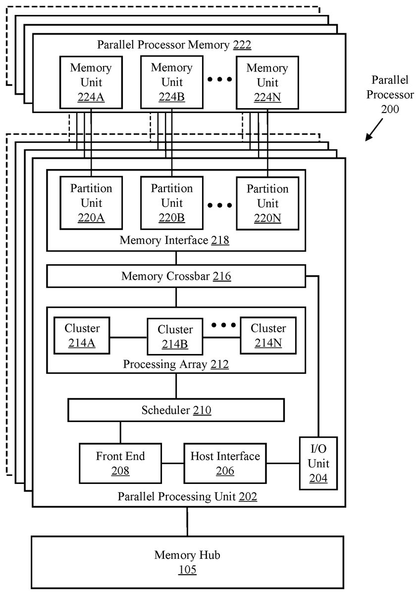
FIG. 2Aillustrates a parallel processor200, according to an embodiment. The various components of the parallel processor200may be implemented using one or more integrated circuit devices, such as programmable processors, application specific integrated circuits (ASICs), or field programmable gate arrays (FPGA). The illustrated parallel processor200is a variant of the one or more parallel processor(s)112shown inFIG. 1, according to an embodiment.
In one embodiment the parallel processor200includes a parallel processing unit202. The parallel processing unit includes an I/O unit204that enables communication with other devices, including other instances of the parallel processing unit202. The I/O unit204may be directly connected to other devices. In one embodiment the I/O unit204connects with other devices via the use of a hub or switch interface, such as memory hub105. The connections between the memory hub105and the I/O unit204form a communication link113. Within the parallel processing unit202, the I/O unit204connects with a host interface206and a memory crossbar216, where the host interface206receives commands directed to performing processing operations and the memory crossbar216receives commands directed to performing memory operations.
When the host interface206receives a command buffer via the I/O unit204, the host interface206can direct work operations to perform those commands to a front end208. In one embodiment the front end208couples with a scheduler210, which is configured to distribute commands or other work items to a processing cluster array212. In one embodiment the scheduler210ensures that the processing cluster array212is properly configured and in a valid state before tasks are distributed to the processing clusters of the processing cluster array212. In one embodiment the scheduler210is implemented via firmware logic executing on a microcontroller. The microcontroller implemented scheduler210is configurable to perform complex scheduling and work distribution operations at coarse and fine granularity, enabling rapid preemption and context switching of threads executing on the processing array212. In one embodiment, the host software can prove workloads for scheduling on the processing array212via one of multiple graphics processing doorbells. The workloads can then be automatically distributed across the processing array212by the scheduler210logic within the scheduler microcontroller.
The processing cluster array212can include up to “N” processing clusters (e.g., cluster214A, cluster214B, through cluster214N). Each cluster214A-214N of the processing cluster array212can execute a large number of concurrent threads. The scheduler210can allocate work to the clusters214A-214N of the processing cluster array212using various scheduling and/or work distribution algorithms, which may vary depending on the workload arising for each type of program or computation. The scheduling can be handled dynamically by the scheduler210, or can be assisted in part by compiler logic during compilation of program logic configured for execution by the processing cluster array212. In one embodiment, different clusters214A-214N of the processing cluster array212can be allocated for processing different types of programs or for performing different types of computations.
The processing cluster array212can be configured to perform various types of parallel processing operations. In one embodiment the processing cluster array212is configured to perform general-purpose parallel compute operations. For example, the processing cluster array212can include logic to execute processing tasks including filtering of video and/or audio data, performing modeling operations, including physics operations, and performing data transformations.
In one embodiment the processing cluster array212is configured to perform parallel graphics processing operations. In embodiments in which the parallel processor200is configured to perform graphics processing operations, the processing cluster array212can include additional logic to support the execution of such graphics processing operations, including, but not limited to texture sampling logic to perform texture operations, as well as tessellation logic and other vertex processing logic. Additionally, the processing cluster array212can be configured to execute graphics processing related shader programs such as, but not limited to vertex shaders, tessellation shaders, geometry shaders, and pixel shaders. The parallel processing unit202can transfer data from system memory via the I/O unit204for processing. During processing the transferred data can be stored to on-chip memory (e.g., parallel processor memory222) during processing, then written back to system memory.
In one embodiment, when the parallel processing unit202is used to perform graphics processing, the scheduler210can be configured to divide the processing workload into approximately equal sized tasks, to better enable distribution of the graphics processing operations to multiple clusters214A-214N of the processing cluster array212. In some embodiments, portions of the processing cluster array212can be configured to perform different types of processing. For example a first portion may be configured to perform vertex shading and topology generation, a second portion may be configured to perform tessellation and geometry shading, and a third portion may be configured to perform pixel shading or other screen space operations, to produce a rendered image for display. Intermediate data produced by one or more of the clusters214A-214N may be stored in buffers to allow the intermediate data to be transmitted between clusters214A-214N for further processing.
During operation, the processing cluster array212can receive processing tasks to be executed via the scheduler210, which receives commands defining processing tasks from front end208. For graphics processing operations, processing tasks can include indices of data to be processed, e.g., surface (patch) data, primitive data, vertex data, and/or pixel data, as well as state parameters and commands defining how the data is to be processed (e.g., what program is to be executed). The scheduler210may be configured to fetch the indices corresponding to the tasks or may receive the indices from the front end208. The front end208can be configured to ensure the processing cluster array212is configured to a valid state before the workload specified by incoming command buffers (e.g., batch-buffers, push buffers, etc.) is initiated.
Each of the one or more instances of the parallel processing unit202can couple with parallel processor memory222. The parallel processor memory222can be accessed via the memory crossbar216, which can receive memory requests from the processing cluster array212as well as the I/O unit204. The memory crossbar216can access the parallel processor memory222via a memory interface218. The memory interface218can include multiple partition units (e.g., partition unit220A, partition unit220B, through partition unit220N) that can each couple to a portion (e.g., memory unit) of parallel processor memory222. In one implementation the number of partition units220A-220N is configured to be equal to the number of memory units, such that a first partition unit220A has a corresponding first memory unit224A, a second partition unit220B has a corresponding memory unit224B, and an Nth partition unit220N has a corresponding Nth memory unit224N. In other embodiments, the number of partition units220A-220N may not be equal to the number of memory devices.
In various embodiments, the memory units224A-224N can include various types of memory devices, including dynamic random access memory (DRAM) or graphics random access memory, such as synchronous graphics random access memory (SGRAM), including graphics double data rate (GDDR) memory. In one embodiment, the memory units224A-224N may also include 3D stacked memory, including but not limited to high bandwidth memory (HBM). Persons skilled in the art will appreciate that the specific implementation of the memory units224A-224N can vary, and can be selected from one of various conventional designs. Render targets, such as frame buffers or texture maps may be stored across the memory units224A-224N, allowing partition units220A-220N to write portions of each render target in parallel to efficiently use the available bandwidth of parallel processor memory222. In some embodiments, a local instance of the parallel processor memory222may be excluded in favor of a unified memory design that utilizes system memory in conjunction with local cache memory.
In one embodiment, any one of the clusters214A-214N of the processing cluster array212can process data that will be written to any of the memory units224A-224N within parallel processor memory222. The memory crossbar216can be configured to transfer the output of each cluster214A-214N to any partition unit220A-220N or to another cluster214A-214N, which can perform additional processing operations on the output. Each cluster214A-214N can communicate with the memory interface218through the memory crossbar216to read from or write to various external memory devices. In one embodiment the memory crossbar216has a connection to the memory interface218to communicate with the I/O unit204, as well as a connection to a local instance of the parallel processor memory222, enabling the processing units within the different processing clusters214A-214N to communicate with system memory or other memory that is not local to the parallel processing unit202. In one embodiment the memory crossbar216can use virtual channels to separate traffic streams between the clusters214A-214N and the partition units220A-220N.
While a single instance of the parallel processing unit202is illustrated within the parallel processor200, any number of instances of the parallel processing unit202can be included. For example, multiple instances of the parallel processing unit202can be provided on a single add-in card, or multiple add-in cards can be interconnected. The different instances of the parallel processing unit202can be configured to inter-operate even if the different instances have different numbers of processing cores, different amounts of local parallel processor memory, and/or other configuration differences. For example and in one embodiment, some instances of the parallel processing unit202can include higher precision floating point units relative to other instances. Systems incorporating one or more instances of the parallel processing unit202or the parallel processor200can be implemented in a variety of configurations and form factors, including but not limited to desktop, laptop, or handheld personal computers, servers, workstations, game consoles, and/or embedded systems.
FIG. 2Bis a block diagram of a partition unit220, according to an embodiment. In one embodiment the partition unit220is an instance of one of the partition units220A-220N ofFIG. 2A. As illustrated, the partition unit220includes an L2cache221, a frame buffer interface225, and a ROP226(raster operations unit). The L2cache221is a read/write cache that is configured to perform load and store operations received from the memory crossbar216and ROP226. Read misses and urgent write-back requests are output by L2cache221to frame buffer interface225for processing. Updates can also be sent to the frame buffer via the frame buffer interface225for processing. In one embodiment the frame buffer interface225interfaces with one of the memory units in parallel processor memory, such as the memory units224A-224N ofFIG. 2(e.g., within parallel processor memory222).
In graphics applications, the ROP226is a processing unit that performs raster operations such as stencil, z test, blending, and the like. The ROP226then outputs processed graphics data that is stored in graphics memory. In some embodiments the ROP226includes compression logic to compress depth or color data that is written to memory and decompress depth or color data that is read from memory. The compression logic can be lossless compression logic that makes use of one or more of multiple compression algorithms. The type of compression that is performed by the ROP226can vary based on the statistical characteristics of the data to be compressed. For example, in one embodiment, delta color compression is performed on depth and color data on a per-tile basis.
In some embodiments, the ROP226is included within each processing cluster (e.g., cluster214A-214N ofFIG. 2) instead of within the partition unit220. In such embodiment, read and write requests for pixel data are transmitted over the memory crossbar216instead of pixel fragment data. The processed graphics data may be displayed on a display device, such as one of the one or more display device(s)110ofFIG. 1, routed for further processing by the processor(s)102, or routed for further processing by one of the processing entities within the parallel processor200ofFIG. 2A.
FIG. 2Cis a block diagram of a processing cluster214within a parallel processing unit, according to an embodiment. In one embodiment the processing cluster is an instance of one of the processing clusters214A-214N ofFIG. 2. The processing cluster214can be configured to execute many threads in parallel, where the term “thread” refers to an instance of a particular program executing on a particular set of input data. In some embodiments, single-instruction, multiple-data (SIMD) instruction issue techniques are used to support parallel execution of a large number of threads without providing multiple independent instruction units. In other embodiments, single-instruction, multiple-thread (SIMT) techniques are used to support parallel execution of a large number of generally synchronized threads, using a common instruction unit configured to issue instructions to a set of processing engines within each one of the processing clusters. Unlike a SIMD execution regime, where all processing engines typically execute identical instructions, SIMT execution allows different threads to more readily follow divergent execution paths through a given thread program. Persons skilled in the art will understand that a SIMD processing regime represents a functional subset of a SIMT processing regime.
Operation of the processing cluster214can be controlled via a pipeline manager232that distributes processing tasks to SIMT parallel processors. The pipeline manager232receives instructions from the scheduler210ofFIG. 2and manages execution of those instructions via a graphics multiprocessor234and/or a texture unit236. The illustrated graphics multiprocessor234is an exemplary instance of a SIMT parallel processor. However, various types of SIMT parallel processors of differing architectures may be included within the processing cluster214. One or more instances of the graphics multiprocessor234can be included within a processing cluster214. The graphics multiprocessor234can process data and a data crossbar240can be used to distribute the processed data to one of multiple possible destinations, including other shader units. The pipeline manager232can facilitate the distribution of processed data by specifying destinations for processed data to be distributed vis the data crossbar240.
Each graphics multiprocessor234within the processing cluster214can include an identical set of functional execution logic (e.g., arithmetic logic units, load-store units, etc.). The functional execution logic can be configured in a pipelined manner in which new instructions can be issued before previous instructions are complete. The functional execution logic supports a variety of operations including integer and floating point arithmetic, comparison operations, Boolean operations, bit-shifting, and computation of various algebraic functions. In one embodiment the same functional-unit hardware can be leveraged to perform different operations and any combination of functional units may be present.
The instructions transmitted to the processing cluster214constitutes a thread. A set of threads executing across the set of parallel processing engines is a thread group. A thread group executes the same program on different input data. Each thread within a thread group can be assigned to a different processing engine within a graphics multiprocessor234. A thread group may include fewer threads than the number of processing engines within the graphics multiprocessor234. When a thread group includes fewer threads than the number of processing engines, one or more of the processing engines may be idle during cycles in which that thread group is being processed. A thread group may also include more threads than the number of processing engines within the graphics multiprocessor234. When the thread group includes more threads than the number of processing engines within the graphics multiprocessor234processing can be performed over consecutive clock cycles. In one embodiment multiple thread groups can be executed concurrently on a graphics multiprocessor234.
In one embodiment the graphics multiprocessor234includes an internal cache memory to perform load and store operations. In one embodiment, the graphics multiprocessor234can forego an internal cache and use a cache memory (e.g., L1cache308) within the processing cluster214. Each graphics multiprocessor234also has access to L2caches within the partition units (e.g., partition units220A-220N ofFIG. 2) that are shared among all processing clusters214and may be used to transfer data between threads. The graphics multiprocessor234may also access off-chip global memory, which can include one or more of local parallel processor memory and/or system memory. Any memory external to the parallel processing unit202may be used as global memory. Embodiments in which the processing cluster214includes multiple instances of the graphics multiprocessor234can share common instructions and data, which may be stored in the L1cache308.
Each processing cluster214may include an MMU245(memory management unit) that is configured to map virtual addresses into physical addresses. In other embodiments, one or more instances of the MMU245may reside within the memory interface218ofFIG. 2. The MMU245includes a set of page table entries (PTEs) used to map a virtual address to a physical address of a tile (talk more about tiling) and optionally a cache line index. The MMU245may include address translation lookaside buffers (TLB) or caches that may reside within the graphics multiprocessor234or the L1cache or processing cluster214. The physical address is processed to distribute surface data access locality to allow efficient request interleaving among partition units. The cache line index may be used to determine whether a request for a cache line is a hit or miss.
In graphics and computing applications, a processing cluster214may be configured such that each graphics multiprocessor234is coupled to a texture unit236for performing texture mapping operations, e.g., determining texture sample positions, reading texture data, and filtering the texture data. Texture data is read from an internal texture L1cache (not shown) or in some embodiments from the L1cache within graphics multiprocessor234and is fetched from an L2cache, local parallel processor memory, or system memory, as needed. Each graphics multiprocessor234outputs processed tasks to the data crossbar240to provide the processed task to another processing cluster214for further processing or to store the processed task in an L2cache, local parallel processor memory, or system memory via the memory crossbar216. A preROP242(pre-raster operations unit) is configured to receive data from graphics multiprocessor234, direct data to ROP units, which may be located with partition units as described herein (e.g., partition units220A-220N ofFIG. 2). The preROP242unit can perform optimizations for color blending, organize pixel color data, and perform address translations.
It will be appreciated that the core architecture described herein is illustrative and that variations and modifications are possible. Any number of processing units, e.g., graphics multiprocessor234, texture units236, preROPs242, etc., may be included within a processing cluster214. Further, while only one processing cluster214is shown, a parallel processing unit as described herein may include any number of instances of the processing cluster214. In one embodiment, each processing cluster214can be configured to operate independently of other processing clusters214using separate and distinct processing units, L1caches, etc.
FIG. 2Dshows a graphics multiprocessor234, according to one embodiment. In such embodiment the graphics multiprocessor234couples with the pipeline manager232of the processing cluster214. The graphics multiprocessor234has an execution pipeline including but not limited to an instruction cache252, an instruction unit254, an address mapping unit256, a register file258, one or more general purpose graphics processing unit (GPGPU) cores262, and one or more load/store units266. The GPGPU cores262and load/store units266are coupled with cache memory272and shared memory270via a memory and cache interconnect268.
In one embodiment, the instruction cache252receives a stream of instructions to execute from the pipeline manager232. The instructions are cached in the instruction cache252and dispatched for execution by the instruction unit254. The instruction unit254can dispatch instructions as thread groups (e.g., warps), with each thread of the thread group assigned to a different execution unit within GPGPU core262. An instruction can access any of a local, shared, or global address space by specifying an address within a unified address space. The address mapping unit256can be used to translate addresses in the unified address space into a distinct memory address that can be accessed by the load/store units266.
The register file258provides a set of registers for the functional units of the graphics multiprocessor324. The register file258provides temporary storage for operands connected to the data paths of the functional units (e.g., GPGPU cores262, load/store units266) of the graphics multiprocessor324. In one embodiment, the register file258is divided between each of the functional units such that each functional unit is allocated a dedicated portion of the register file258. In one embodiment, the register file258is divided between the different warps being executed by the graphics multiprocessor324.
The GPGPU cores262can each include floating point units (FPUs) and/or integer arithmetic logic units (ALUs) that are used to execute instructions of the graphics multiprocessor324. The GPGPU cores262can be similar in architecture or can differ in architecture, according to embodiments. For example and in one embodiment, a first portion of the GPGPU cores262include a single precision FPU and an integer ALU while a second portion of the GPGPU cores include a double precision FPU. In one embodiment the FPUs can implement the IEEE 754-2008 standard for floating point arithmetic or enable variable precision floating point arithmetic. The graphics multiprocessor324can additionally include one or more fixed function or special function units to perform specific functions such as copy rectangle or pixel blending operations. In one embodiment one or more of the GPGPU cores can also include fixed or special function logic.
In one embodiment the GPGPU cores262include SIMD logic capable of performing a single instruction on multiple sets of data. In one embodiment GPGPU cores262can physically execute SIMD4, SIMD8, and SIMD16 instructions and logically execute SIMD1, SIMD2, and SIMD32 instructions. The SIMD instructions for the GPGPU cores can be generated at compile time by a shader compiler or automatically generated when executing programs written and compiled for single program multiple data (SPMD) or SIMT architectures. Multiple threads of a program configured for the SIMT execution model can executed via a single SIMD instruction. For example and in one embodiment, eight SIMT threads that perform the same or similar operations can be executed in parallel via a single SIMD8 logic unit.
The memory and cache interconnect268is an interconnect network that connects each of the functional units of the graphics multiprocessor324to the register file258and to the shared memory270. In one embodiment, the memory and cache interconnect268is a crossbar interconnect that allows the load/store unit266to implement load and store operations between the shared memory270and the register file258. The register file258can operate at the same frequency as the GPGPU cores262, thus data transfer between the GPGPU cores262and the register file258is very low latency. The shared memory270can be used to enable communication between threads that execute on the functional units within the graphics multiprocessor234. The cache memory272can be used as a data cache for example, to cache texture data communicated between the functional units and the texture unit236. The shared memory270can also be used as a program managed cached. Threads executing on the GPGPU cores262can programmatically store data within the shared memory in addition to the automatically cached data that is stored within the cache memory272.
FIGS. 3A-3Billustrate additional graphics multiprocessors, according to embodiments. The illustrated graphics multiprocessors325,350are variants of the graphics multiprocessor234ofFIG. 2C. The illustrated graphics multiprocessors325,350can be configured as a streaming multiprocessor (SM) capable of simultaneous execution of a large number of execution threads.
FIG. 3Ashows a graphics multiprocessor325according to an additional embodiment. The graphics multiprocessor325includes multiple additional instances of execution resource units relative to the graphics multiprocessor234ofFIG. 2D. For example, the graphics multiprocessor325can include multiple instances of the instruction unit332A-332B, register file334A-334B, and texture unit(s)344A-344B. The graphics multiprocessor325also includes multiple sets of graphics or compute execution units (e.g., GPGPU core336A-336B, GPGPU core337A-337B, GPGPU core338A-338B) and multiple sets of load/store units340A-340B. In one embodiment the execution resource units have a common instruction cache330, texture and/or data cache memory342, and shared memory346.
The various components can communicate via an interconnect fabric327. In one embodiment the interconnect fabric327includes one or more crossbar switches to enable communication between the various components of the graphics multiprocessor325. In one embodiment the interconnect fabric327is a separate, high-speed network fabric layer upon which each component of the graphics multiprocessor325is stacked. The components of the graphics multiprocessor325communicate with remote components via the interconnect fabric327. For example, the GPGPU cores336A-336B,337A-337B, and3378A-338B can each communicate with shared memory346via the interconnect fabric327. The interconnect fabric327can arbitrate communication within the graphics multiprocessor325to ensure a fair bandwidth allocation between components.
FIG. 3Bshows a graphics multiprocessor350according to an additional embodiment. The graphics processor includes multiple sets of execution resources356A-356D, where each set of execution resource includes multiple instruction units, register files, GPGPU cores, and load store units, as illustrated inFIG. 2DandFIG. 3A. The execution resources356A-356D can work in concert with texture unit(s)360A-360D for texture operations, while sharing an instruction cache354, and shared memory362. In one embodiment the execution resources356A-356D can share an instruction cache354and shared memory362, as well as multiple instances of a texture and/or data cache memory358A-358B. The various components can communicate via an interconnect fabric352similar to the interconnect fabric327ofFIG. 3A.
Persons skilled in the art will understand that the architecture described inFIGS. 1, 2A-2D, and 3A-3Bare descriptive and not limiting as to the scope of the present embodiments. Thus, the techniques described herein may be implemented on any properly configured processing unit, including, without limitation, one or more mobile application processors, one or more desktop or server central processing units (CPUs) including multi-core CPUs, one or more parallel processing units, such as the parallel processing unit202ofFIG. 2, as well as one or more graphics processors or special purpose processing units, without departure from the scope of the embodiments described herein.
In some embodiments a parallel processor or GPGPU as described herein is communicatively coupled to host/processor cores to accelerate graphics operations, machine-learning operations, pattern analysis operations, and various general purpose GPU (GPGPU) functions. The GPU may be communicatively coupled to the host processor/cores over a bus or other interconnect (e.g., a high speed interconnect such as PCIe or NVLink). In other embodiments, the GPU may be integrated on the same package or chip as the cores and communicatively coupled to the cores over an internal processor bus/interconnect (i.e., internal to the package or chip). Regardless of the manner in which the GPU is connected, the processor cores may allocate work to the GPU in the form of sequences of commands/instructions contained in a work descriptor. The GPU then uses dedicated circuitry/logic for efficiently processing these commands/instructions.
Techniques for GPU to Host Processor Interconnection
FIG. 4Aillustrates an exemplary architecture in which a plurality of GPUs410-413are communicatively coupled to a plurality of multi-core processors405-406over high-speed links440-443(e.g., buses, point-to-point interconnects, etc.). In one embodiment, the high-speed links440-443support a communication throughput of 4 GB/s, 30 GB/s, 80 GB/s or higher, depending on the implementation. Various interconnect protocols may be used including, but not limited to, PCIe 4.0 or 5.0 and NVLink 2.0. However, the underlying principles of the invention are not limited to any particular communication protocol or throughput.
In addition, in one embodiment, two or more of the GPUs410-413are interconnected over high-speed links444-445, which may be implemented using the same or different protocols/links than those used for high-speed links440-443. Similarly, two or more of the multi-core processors405-406may be connected over high speed link433which may be symmetric multi-processor (SMP) buses operating at 20 GB/s, 30 GB/s, 120GB/s or higher. Alternatively, all communication between the various system components shown inFIG. 4Amay be accomplished using the same protocols/links (e.g., over a common interconnection fabric). As mentioned, however, the underlying principles of the invention are not limited to any particular type of interconnect technology.
In one embodiment, each multi-core processor405-406is communicatively coupled to a processor memory401-402, via memory interconnects430-431, respectively, and each GPU410-413is communicatively coupled to GPU memory420-423over GPU memory interconnects450-453, respectively. The memory interconnects430-431and450-453may utilize the same or different memory access technologies. By way of example, and not limitation, the processor memories401-402and GPU memories420-423may be volatile memories such as dynamic random access memories (DRAMs) (including stacked DRAMs), Graphics DDR SDRAM (GDDR) (e.g., GDDR5, GDDR6), or High Bandwidth Memory (HBM) and/or may be non-volatile memories such as 3D XPoint or Nano-Ram. In one embodiment, some portion of the memories may be volatile memory and another portion may be non-volatile memory (e.g., using a two-level memory (2LM) hierarchy).
As described below, although the various processors405-406and GPUs410-413may be physically coupled to a particular memory401-402,420-423, respectively, a unified memory architecture may be implemented in which the same virtual system address space (also referred to as the “effective address” space) is distributed among all of the various physical memories. For example, processor memories401-402may each comprise 64 GB of the system memory address space and GPU memories420-423may each comprise 32 GB of the system memory address space (resulting in a total of 256 GB addressable memory in this example).
FIG. 4Billustrates additional details for an interconnection between a multi-core processor407and a graphics acceleration module446in accordance with one embodiment. The graphics acceleration module446may include one or more GPU chips integrated on a line card which is coupled to the processor407via the high-speed link440. Alternatively, the graphics acceleration module446may be integrated on the same package or chip as the processor407.
The illustrated processor407includes a plurality of cores460A-460D, each with a translation lookaside buffer461A-461D and one or more caches462A-462D. The cores may include various other components for executing instructions and processing data which are not illustrated to avoid obscuring the underlying principles of the invention (e.g., instruction fetch units, branch prediction units, decoders, execution units, reorder buffers, etc.). The caches462A-462D may comprise level 1 (L1) and level 2 (L2) caches. In addition, one or more shared caches426may be included in the caching hierarchy and shared by sets of the cores460A-460D. For example, one embodiment of the processor407includes24cores, each with its own L1cache, twelve shared L2caches, and twelve shared L3caches. In this embodiment, one of the L2and L3caches are shared by two adjacent cores. The processor407and the graphics accelerator integration module446connect with system memory441, which may include processor memories401-402
Coherency is maintained for data and instructions stored in the various caches462A-462D,456and system memory441via inter-core communication over a coherence bus464. For example, each cache may have cache coherency logic/circuitry associated therewith to communicate to over the coherence bus464in response to detected reads or writes to particular cache lines. In one implementation, a cache snooping protocol is implemented over the coherence bus464to snoop cache accesses. Cache snooping/coherency techniques are well understood by those of skill in the art and will not be described in detail here to avoid obscuring the underlying principles of the invention.
In one embodiment, a proxy circuit425communicatively couples the graphics acceleration module446to the coherence bus464, allowing the graphics acceleration module446to participate in the cache coherence protocol as a peer of the cores. In particular, an interface435provides connectivity to the proxy circuit425over high-speed link440(e.g., a PCIe bus, NVLink, etc.) and an interface437connects the graphics acceleration module446to the link440.
In one implementation, an accelerator integration circuit436provides cache management, memory access, context management, and interrupt management services on behalf of a plurality of graphics processing engines431,432, N of the graphics acceleration module446. The graphics processing engines431,432, N may each comprise a separate graphics processing unit (GPU). Alternatively, the graphics processing engines431,432, N may comprise different types of graphics processing engines within a GPU such as graphics execution units, media processing engines (e.g., video encoders/decoders), samplers, and blit engines. In other words, the graphics acceleration module may be a GPU with a plurality of graphics processing engines431-432, N or the graphics processing engines431-432, N may be individual GPUs integrated on a common package, line card, or chip.
In one embodiment, the accelerator integration circuit436includes a memory management unit (MMU)439for performing various memory management functions such as virtual-to-physical memory translations (also referred to as effective-to-real memory translations) and memory access protocols for accessing system memory441. The MMU439may also include a translation lookaside buffer (TLB) (not shown) for caching the virtual/effective to physical/real address translations. In one implementation, a cache438stores commands and data for efficient access by the graphics processing engines431-432, N. In one embodiment, the data stored in cache438and graphics memories433-434, N is kept coherent with the core caches462A-462D,456and system memory411. As mentioned, this may be accomplished via proxy circuit425which takes part in the cache coherency mechanism on behalf of cache438and memories433-434, N (e.g., sending updates to the cache438related to modifications/accesses of cache lines on processor caches462A-462D,456and receiving updates from the cache438).
A set of registers445store context data for threads executed by the graphics processing engines431-432, N and a context management circuit448manages the thread contexts. For example, the context management circuit448may perform save and restore operations to save and restore contexts of the various threads during contexts switches (e.g., where a first thread is saved and a second thread is stored so that the second thread can be execute by a graphics processing engine). For example, on a context switch, the context management circuit448may store current register values to a designated region in memory (e.g., identified by a context pointer). It may then restore the register values when returning to the context. In one embodiment, an interrupt management circuit447receives and processes interrupts received from system devices.
In one implementation, virtual/effective addresses from a graphics processing engine431are translated to real/physical addresses in system memory411by the MMU439. One embodiment of the accelerator integration circuit436supports multiple (e.g., 4, 8, 16) graphics accelerator modules446and/or other accelerator devices. The graphics accelerator module446may be dedicated to a single application executed on the processor407or may be shared between multiple applications. In one embodiment, a virtualized graphics execution environment is presented in which the resources of the graphics processing engines431-432, N are shared with multiple applications or virtual machines (VMs). The resources may be subdivided into “slices” which are allocated to different VMs and/or applications based on the processing requirements and priorities associated with the VMs and/or applications.
Thus, the accelerator integration circuit acts as a bridge to the system for the graphics acceleration module446and provides address translation and system memory cache services. In addition, the accelerator integration circuit436may provide virtualization facilities for the host processor to manage virtualization of the graphics processing engines, interrupts, and memory management.
Because hardware resources of the graphics processing engines431-432, N are mapped explicitly to the real address space seen by the host processor407, any host processor can address these resources directly using an effective address value. One function of the accelerator integration circuit436, in one embodiment, is the physical separation of the graphics processing engines431-432, N so that they appear to the system as independent units.
As mentioned, in the illustrated embodiment, one or more graphics memories433-434, M are coupled to each of the graphics processing engines431-432, N, respectively. The graphics memories433-434, M store instructions and data being processed by each of the graphics processing engines431-432, N. The graphics memories433-434, M may be volatile memories such as DRAMs (including stacked DRAMs), GDDR memory (e.g., GDDR5, GDDR6), or HBM, and/or may be non-volatile memories such as 3D XPoint or Nano-Ram.
In one embodiment, to reduce data traffic over link440, biasing techniques are used to ensure that the data stored in graphics memories433-434, M is data which will be used most frequently by the graphics processing engines431-432, N and preferably not used by the cores460A-460D (at least not frequently). Similarly, the biasing mechanism attempts to keep data needed by the cores (and preferably not the graphics processing engines431-432, N) within the caches462A-462D,456of the cores and system memory411.
FIG. 4Cillustrates another embodiment in which the accelerator integration circuit436is integrated within the processor407. In this embodiment, the graphics processing engines431-432, N communicate directly over the high-speed link440to the accelerator integration circuit436via interface437and interface435(which, again, may be utilize any form of bus or interface protocol). The accelerator integration circuit436may perform the same operations as those described with respect toFIG. 4B, but potentially at a higher throughput given its close proximity to the coherency bus462and caches462A-462D,426.
One embodiment supports different programming models including a dedicated-process programming model (no graphics acceleration module virtualization) and shared programming models (with virtualization). The latter may include programming models which are controlled by the accelerator integration circuit436and programming models which are controlled by the graphics acceleration module446.
In one embodiment of the dedicated process model, graphics processing engines431-432, N are dedicated to a single application or process under a single operating system. The single application can funnel other application requests to the graphics engines431-432, N, providing virtualization within a VM/partition.
In the dedicated-process programming models, the graphics processing engines431-432, N, may be shared by multiple VM/application partitions. The shared models require a system hypervisor to virtualize the graphics processing engines431-432, N to allow access by each operating system. For single-partition systems without a hypervisor, the graphics processing engines431-432, N are owned by the operating system. In both cases, the operating system can virtualize the graphics processing engines431-432, N to provide access to each process or application.
For the shared programming model, the graphics acceleration module446or an individual graphics processing engine431-432, N selects a process element using a process handle. In one embodiment, process elements are stored in system memory411and are addressable using the effective address to real address translation techniques described herein. The process handle may be an implementation-specific value provided to the host process when registering its context with the graphics processing engine431-432, N (that is, calling system software to add the process element to the process element linked list). The lower16-bits of the process handle may be the offset of the process element within the process element linked list.
FIG. 4Dillustrates an exemplary accelerator integration slice490. As used herein, a “slice” comprises a specified portion of the processing resources of the accelerator integration circuit436. Application effective address space482within system memory411stores process elements483. In one embodiment, the process elements483are stored in response to GPU invocations481from applications480executed on the processor407. A process element483contains the process state for the corresponding application480. A work descriptor (WD)484contained in the process element483can be a single job requested by an application or may contain a pointer to a queue of jobs. In the latter case, the WD484is a pointer to the job request queue in the application's address space482.
The graphics acceleration module446and/or the individual graphics processing engines431-432, N can be shared by all or a subset of the processes in the system. Embodiments of the invention include an infrastructure for setting up the process state and sending a WD484to a graphics acceleration module446to start a job in a virtualized environment.
In one implementation, the dedicated-process programming model is implementation-specific. In this model, a single process owns the graphics acceleration module446or an individual graphics processing engine431. Because the graphics acceleration module446is owned by a single process, the hypervisor initializes the accelerator integration circuit436for the owning partition and the operating system initializes the accelerator integration circuit436for the owning process at the time when the graphics acceleration module446is assigned.
In operation, a WD fetch unit491in the accelerator integration slice490fetches the next WD484which includes an indication of the work to be done by one of the graphics processing engines of the graphics acceleration module446. Data from the WD484may be stored in registers445and used by the MMU439, interrupt management circuit447and/or context management circuit446as illustrated. For example, one embodiment of the MMU439includes segment/page walk circuitry for accessing segment/page tables486within the OS virtual address space485. The interrupt management circuit447may process interrupt events492received from the graphics acceleration module446. When performing graphics operations, an effective address493generated by a graphics processing engine431-432, N is translated to a real address by the MMU439.
In one embodiment, the same set of registers445are duplicated for each graphics processing engine431-432, N and/or graphics acceleration module446and may be initialized by the hypervisor or operating system. Each of these duplicated registers may be included in an accelerator integration slice490. Exemplary registers that may be initialized by the hypervisor are shown in Table 1.
TABLE 1Hypervisor Initialized Registers1Slice Control Register2Real Address (RA) Scheduled Processes Area Pointer3Authority Mask Override Register4Interrupt Vector Table Entry Offset5Interrupt Vector Table Entry Limit6State Register7Logical Partition ID8Real address (RA) Hypervisor Accelerator Utilization RecordPointer9Storage Description Register
Exemplary registers that may be initialized by the operating system are shown in Table 2.
TABLE 2Operating System Initialized Registers1Process and Thread Identification2Effective Address (EA) Context Save/Restore Pointer3Virtual Address (VA) Accelerator Utilization Record Pointer4Virtual Address (VA) Storage Segment Table Pointer5Authority Mask6Work descriptor
In one embodiment, each WD484is specific to a particular graphics acceleration module446and/or graphics processing engine431-432, N. It contains all the information a graphics processing engine431-432, N requires to do its work or it can be a pointer to a memory location where the application has set up a command queue of work to be completed.
FIG. 4Eillustrates additional details for one embodiment of a shared model. This embodiment includes a hypervisor real address space498in which a process element list499is stored. The hypervisor real address space498is accessible via a hypervisor496which virtualizes the graphics acceleration module engines for the operating system495.
The shared programming models allow for all or a subset of processes from all or a subset of partitions in the system to use a graphics acceleration module446. There are two programming models where the graphics acceleration module446is shared by multiple processes and partitions: time-sliced shared and graphics directed shared.
In this model, the system hypervisor496owns the graphics acceleration module446and makes its function available to all operating systems495. For a graphics acceleration module446to support virtualization by the system hypervisor496, the graphics acceleration module446may adhere to the following requirements: 1) An application's job request must be autonomous (that is, the state does not need to be maintained between jobs), or the graphics acceleration module446must provide a context save and restore mechanism. 2) An application's job request is guaranteed by the graphics acceleration module446to complete in a specified amount of time, including any translation faults, or the graphics acceleration module446provides the ability to preempt the processing of the job. 3) The graphics acceleration module446must be guaranteed fairness between processes when operating in the directed shared programming model.
In one embodiment, for the shared model, the application480is required to make an operating system495system call with a graphics acceleration module446type, a work descriptor (WD), an authority mask register (AMR) value, and a context save/restore area pointer (CSRP). The graphics acceleration module446type describes the targeted acceleration function for the system call. The graphics acceleration module446type may be a system-specific value. The WD is formatted specifically for the graphics acceleration module446and can be in the form of a graphics acceleration module446command, an effective address pointer to a user-defined structure, an effective address pointer to a queue of commands, or any other data structure to describe the work to be done by the graphics acceleration module446. In one embodiment, the AMR value is the AMR state to use for the current process. The value passed to the operating system is similar to an application setting the AMR. If the accelerator integration circuit436and graphics acceleration module446implementations do not support a User Authority Mask Override Register (UAMOR), the operating system may apply the current UAMOR value to the AMR value before passing the AMR in the hypervisor call. The hypervisor496may optionally apply the current Authority Mask Override Register (AMOR) value before placing the AMR into the process element483. In one embodiment, the CSRP is one of the registers445containing the effective address of an area in the application's address space482for the graphics acceleration module446to save and restore the context state. This pointer is optional if no state is required to be saved between jobs or when a job is preempted. The context save/restore area may be pinned system memory.
Upon receiving the system call, the operating system495may verify that the application480has registered and been given the authority to use the graphics acceleration module446. The operating system495then calls the hypervisor496with the information shown in Table 3.
TABLE 3OS to Hypervisor Call Parameters1A work descriptor (WD)2An Authority Mask Register (AMR) value (potentially masked).3An effective address (EA) Context Save/Restore Area Pointer(CSRP)4A process ID (PID) and optional thread ID (TID)5A virtual address (VA) accelerator utilization record pointer(AURP)6The virtual address of the storage segment table pointer (SSTP)7A logical interrupt service number (LISN)
Upon receiving the hypervisor call, the hypervisor496verifies that the operating system495has registered and been given the authority to use the graphics acceleration module446. The hypervisor496then puts the process element483into the process element linked list for the corresponding graphics acceleration module446type. The process element may include the information shown in Table4.
TABLE 4Process Element Information1A work descriptor (WD)2An Authority Mask Register (AMR) value (potentially masked).3An effective address (EA) Context Save/Restore Area Pointer(CSRP)4A process ID (PID) and optional thread ID (TID)5A virtual address (VA) accelerator utilization record pointer(AURP)6The virtual address of the storage segment table pointer (SSTP)7A logical interrupt service number (LISN)8Interrupt vector table, derived from the hypervisor call parameters.9A state register (SR) value10A logical partition ID (LPID)11A real address (RA) hypervisor accelerator utilization recordpointer12The Storage Descriptor Register (SDR)
In one embodiment, the hypervisor initializes a plurality of accelerator integration slice490registers445.
As illustrated inFIG. 4F, one embodiment of the invention employs a unified memory addressable via a common virtual memory address space used to access the physical processor memories401-402and GPU memories420-423. In this implementation, operations executed on the GPUs410-413utilize the same virtual/effective memory address space to access the processors memories401-402and vice versa, thereby simplifying programmability. In one embodiment, a first portion of the virtual/effective address space is allocated to the processor memory401, a second portion to the second processor memory402, a third portion to the GPU memory420, and so on. The entire virtual/effective memory space (sometimes referred to as the effective address space) is thereby distributed across each of the processor memories401-402and GPU memories420-423, allowing any processor or GPU to access any physical memory with a virtual address mapped to that memory.
In one embodiment, bias/coherence management circuitry494A-494E within one or more of the MMUs439A-439E ensures cache coherence between the caches of the host processors (e.g.,405) and the GPUs410-413and implements biasing techniques indicating the physical memories in which certain types of data should be stored. While multiple instances of bias/coherence management circuitry494A-494E are illustrated inFIG. 4F, the bias/coherence circuitry may be implemented within the MMU of one or more host processors405and/or within the accelerator integration circuit436.
One embodiment allows GPU-attached memory420-423to be mapped as part of system memory, and accessed using shared virtual memory (SVM) technology, but without suffering the typical performance drawbacks associated with full system cache coherence. The ability to GPU-attached memory420-423to be accessed as system memory without onerous cache coherence overhead provides a beneficial operating environment for GPU offload. This arrangement allows the host processor405software to setup operands and access computation results, without the overhead of tradition I/O DMA data copies. Such traditional copies involve driver calls, interrupts and memory mapped I/O (MMIO) accesses that are all inefficient relative to simple memory accesses. At the same time, the ability to access GPU attached memory420-423without cache coherence overheads can be critical to the execution time of an offloaded computation. In cases with substantial streaming write memory traffic, for example, cache coherence overhead can significantly reduce the effective write bandwidth seen by a GPU410-413. The efficiency of operand setup, the efficiency of results access, and the efficiency of GPU computation all play a role in determining the effectiveness of GPU offload.
In one implementation, the selection of between GPU bias and host processor bias is driven by a bias tracker data structure. A bias table may be used, for example, which may be a page-granular structure (i.e., controlled at the granularity of a memory page) that includes 1 or 2 bits per GPU-attached memory page. The bias table may be implemented in a stolen memory range of one or more GPU-attached memories420-423, with or without a bias cache in the GPU410-413(e.g., to cache frequently/recently used entries of the bias table). Alternatively, the entire bias table may be maintained within the GPU.
In one implementation, the bias table entry associated with each access to the GPU-attached memory420-423is accessed prior the actual access to the GPU memory, causing the following operations. First, local requests from the GPU410-413that find their page in GPU bias are forwarded directly to a corresponding GPU memory420-423. Local requests from the GPU that find their page in host bias are forwarded to the processor405(e.g., over a high-speed link as discussed above). In one embodiment, requests from the processor405that find the requested page in host processor bias complete the request like a normal memory read. Alternatively, requests directed to a GPU-biased page may be forwarded to the GPU410-413. The GPU may then transition the page to a host processor bias if it is not currently using the page.
The bias state of a page can be changed either by a software-based mechanism, a hardware-assisted software-based mechanism, or, for a limited set of cases, a purely hardware-based mechanism.
One mechanism for changing the bias state employs an API call (e.g. OpenCL), which, in turn, calls the GPU's device driver which, in turn, sends a message (or enqueues a command descriptor) to the GPU directing it to change the bias state and, for some transitions, perform a cache flushing operation in the host. The cache flushing operation is required for a transition from host processor405bias to GPU bias, but is not required for the opposite transition.
In one embodiment, cache coherency is maintained by temporarily rendering GPU-biased pages uncacheable by the host processor405. To access these pages, the processor405may request access from the GPU410which may or may not grant access right away, depending on the implementation. Thus, to reduce communication between the processor405and GPU410it is beneficial to ensure that GPU-biased pages are those which are required by the GPU but not the host processor405and vice versa.
Graphics Processing Pipeline
FIG. 5illustrates a graphics processing pipeline500, according to an embodiment. In one embodiment a graphics processor can implement the illustrated graphics processing pipeline500. The graphics processor can be included within the parallel processing subsystems as described herein, such as the parallel processor200ofFIG. 2, which, in one embodiment, is a variant of the parallel processor(s)112ofFIG. 1. The various parallel processing systems can implement the graphics processing pipeline500via one or more instances of the parallel processing unit (e.g., parallel processing unit202ofFIG. 2) as described herein. For example, a shader unit (e.g., graphics multiprocessor234ofFIG. 3) may be configured to perform the functions of one or more of a vertex processing unit504, a tessellation control processing unit508, a tessellation evaluation processing unit512, a geometry processing unit516, and a fragment/pixel processing unit524. The functions of data assembler502, primitive assemblers506,514,518, tessellation unit510, rasterizer522, and raster operations unit526may also be performed by other processing engines within a processing cluster (e.g., processing cluster214ofFIG. 3) and a corresponding partition unit (e.g., partition unit220A-220N ofFIG. 2). The graphics processing pipeline500may also be implemented using dedicated processing units for one or more functions. In one embodiment, one or more portions of the graphics processing pipeline500can be performed by parallel processing logic within a general purpose processor (e.g., CPU). In one embodiment, one or more portions of the graphics processing pipeline500can access on-chip memory (e.g., parallel processor memory222as inFIG. 2) via a memory interface528, which may be an instance of the memory interface218ofFIG. 2.
In one embodiment the data assembler502is a processing unit that collects vertex data for surfaces and primitives. The data assembler502then outputs the vertex data, including the vertex attributes, to the vertex processing unit504. The vertex processing unit504is a programmable execution unit that executes vertex shader programs, lighting and transforming vertex data as specified by the vertex shader programs. The vertex processing unit504reads data that is stored in cache, local or system memory for use in processing the vertex data and may be programmed to transform the vertex data from an object-based coordinate representation to a world space coordinate space or a normalized device coordinate space.
A first instance of a primitive assembler506receives vertex attributes from the vertex processing unit504. The primitive assembler506readings stored vertex attributes as needed and constructs graphics primitives for processing by tessellation control processing unit508. The graphics primitives include triangles, line segments, points, patches, and so forth, as supported by various graphics processing application programming interfaces (APIs).
The tessellation control processing unit508treats the input vertices as control points for a geometric patch. The control points are transformed from an input representation from the patch (e.g., the patch's bases) to a representation that is suitable for use in surface evaluation by the tessellation evaluation processing unit512. The tessellation control processing unit508can also compute tessellation factors for edges of geometric patches. A tessellation factor applies to a single edge and quantifies a view-dependent level of detail associated with the edge. A tessellation unit510is configured to receive the tessellation factors for edges of a patch and to tessellate the patch into multiple geometric primitives such as line, triangle, or quadrilateral primitives, which are transmitted to a tessellation evaluation processing unit512. The tessellation evaluation processing unit512operates on parameterized coordinates of the subdivided patch to generate a surface representation and vertex attributes for each vertex associated with the geometric primitives.
A second instance of a primitive assembler514receives vertex attributes from the tessellation evaluation processing unit512, reading stored vertex attributes as needed, and constructs graphics primitives for processing by the geometry processing unit516. The geometry processing unit516is a programmable execution unit that executes geometry shader programs to transform graphics primitives received from primitive assembler514as specified by the geometry shader programs. In one embodiment the geometry processing unit516is programmed to subdivide the graphics primitives into one or more new graphics primitives and calculate parameters used to rasterize the new graphics primitives.
In some embodiments the geometry processing unit516can add or delete elements in the geometry stream. The geometry processing unit516outputs the parameters and vertices specifying new graphics primitives to primitive assembler518. The primitive assembler518receives the parameters and vertices from the geometry processing unit516and constructs graphics primitives for processing by a viewport scale, cull, and clip unit520. The geometry processing unit516reads data that is stored in parallel processor memory or system memory for use in processing the geometry data. The viewport scale, cull, and clip unit520performs clipping, culling, and viewport scaling and outputs processed graphics primitives to a rasterizer522.
The rasterizer522can perform depth culling and other depth-based optimizations. The rasterizer522also performs scan conversion on the new graphics primitives to generate fragments and output those fragments and associated coverage data to the fragment/pixel processing unit524. The fragment/pixel processing unit524is a programmable execution unit that is configured to execute fragment shader programs or pixel shader programs. The fragment/pixel processing unit524transforming fragments or pixels received from rasterizer522, as specified by the fragment or pixel shader programs. For example, the fragment/pixel processing unit524may be programmed to perform operations included but not limited to texture mapping, shading, blending, texture correction and perspective correction to produce shaded fragments or pixels that are output to a raster operations unit526. The fragment/pixel processing unit524can read data that is stored in either the parallel processor memory or the system memory for use when processing the fragment data. Fragment or pixel shader programs may be configured to shade at sample, pixel, tile, or other granularities depending on the sampling rate configured for the processing units.
The raster operations unit526is a processing unit that performs raster operations including, but not limited to stencil, z test, blending, and the like, and outputs pixel data as processed graphics data to be stored in graphics memory (e.g., parallel processor memory222as inFIG. 2, and/or system memory104as inFIG. 1, to be displayed on the one or more display device(s)110or for further processing by one of the one or more processor(s)102or parallel processor(s)112. In some embodiments the raster operations unit526is configured to compress z or color data that is written to memory and decompress z or color data that is read from memory.
Shared Computational Work in Cloud Server
FIG. 6illustrates a cloud gaming system600that includes a cloud server602configured, for example, to store, execute, render, and transmit one or more graphics (i.e., game) applications via a network604to one or more users of a corresponding client device606for use during a gaming session. The client device606may be a computing device, including but not limited to desktop computers, laptop computers, smart phones, handheld personal computers, workstations, game consoles, cellular phones, mobile devices, wearable computing devices, tablet computers, convertible tablet computers, or any other electronic, microelectronic, or micro-electromechanical device for processing and communicating data.
FIG. 7shows a computing system700, according to an embodiment. In the illustrated example, a host processor702includes an integrated memory controller (IMC)704that communicates with a system memory706(e.g., DRAM). The host processor702may be coupled to a graphics processor708, which may include a graphics pipeline716, and an input/output (IO) module710. The illustrated graphics processor708is also coupled to a dedicated graphics memory722. The IO module710may be coupled to a network controller712(e.g., wireless and/or wired), a display714(e.g., fixed or head mounted liquid crystal display/LCD, light emitting diode/LED display, etc., to visually present a video of a 3D scene) and mass storage718(e.g., flash memory, optical disk, solid state drive/SSD). According to embodiments, the graphics memory722may be dedicated as illustrated, or alternatively, may be shared with the host processor702.
The system memory706and/or the mass storage718may include instructions720a,720bwhich when executed by the host processor702, cause the host processor702to generate an object description associated with the visual content to be presented by the display714. Additionally, the graphics pipeline716of the graphics processor708may include control architecture that performs one or more aspects of the method900(FIG. 9) and/or the method1000(FIG. 10). Thus, the graphics pipeline716may be configured to detect an initiation of a gaming session by a user via a client device (e.g., a client device606illustrated inFIG. 6and described herein). The gaming session may be conducted, for example, in a virtual gaming environment.
The graphics pipeline716may be configured identify, from graphics data stored in memory706, redundant graphics calculations relating to common frame characteristics of one or more graphical scenes to be shared between the client game devices of users participating in the gaming session. According to embodiments, identifying redundant calculations includes analyzing the graphics data to detect view-independent graphics calculations. As an example, such common frame characteristics may include, but are not limited to, frame geometry and frame shading.
The graphics pipeline716may be configured calculate, in response to the identified redundant graphics calculations, frame characteristics relating to the one or more graphical scenes, and then send, over the computer network, the calculation of the frame characteristics to the client game devices to be visually presented by the client device as rendered visual content in a 3D virtual space. Meaning, instead of performing graphics calculations for each respective client device participating in the gaming session, the graphics pipeline716according to embodiments is to conduct a single calculation for common frame characteristics that are to be shared between the client devices during the gaming session.
According to an embodiment, the graphics pipeline716may be configured to identify, in response to receiving the graphics data, redundant texture maps relating to common frame characteristics of one or more graphical scenes to be shared between the client devices, and generate, in response to the identified redundant texture maps, texture maps relating to the one or more graphical scenes. The graphics pipeline716may be configured to send, over the computer network, the generated texture maps to the client game devices to be visually presented as rendered visual content in a 3D virtual space. According to embodiments, rasterization and pixel shading operations may be performed at each respective client device.
FIG. 8illustrates a diagram of a cloud server apparatus800(e.g., chip) that includes a substrate802(e.g., silicon, sapphire, gallium arsenide) and logic804(804a-804c, e.g., transistor array and other integrated circuit/IC components) operatively coupled to the substrate802. The logic804, which may be implemented in configurable logic and/or fixed-functionality logic hardware, includes a graphics processor804a, a host processor804band an IO module804c. The logic804may generally implement one or more aspects of the method900(FIG. 9) and/or the method1000(FIG,10). Thus, the logic804may be configured to detect an initiation of a gaming session by a user via a client device (e.g., a client device606illustrated inFIG. 6and described herein). The gaming session may be conducted, for example, in a virtual gaming environment.
The logic804may be configured identify, from graphics data stored in memory, redundant graphics calculations relating to common frame characteristics of one or more graphical scenes to be shared between the client game devices of users participating in the gaming session. According to embodiments, identifying redundant calculations includes analyzing the graphics data to detect view-independent graphics calculations. As an example, such common frame characteristics may include, but are not limited to, frame geometry and frame shading.
The logic804may be configured calculate, in response to the identified redundant graphics calculations, frame characteristics relating to the one or more graphical scenes, and then send, over a computer network, the calculation of the frame characteristics to the client game devices to be visually presented by the client device as rendered visual content in a 3D virtual space. Meaning, instead of performing graphics calculations for each respective client device participating in the gaming session, the logic804according to embodiments is to conduct a single calculation for common frame characteristics that are to be shared between the client devices during the gaming session.
According to an embodiment, the logic804may be configured to identify, in response to receiving the graphics data, redundant texture maps relating to common frame characteristics of one or more graphical scenes to be shared between the client devices, and generate, in response to the identified redundant texture maps, texture maps relating to the one or more graphical scenes. According to embodiments, identifying redundant calculations includes analyzing the graphics data to detect view-independent graphics calculations. The logic804may be configured to send, over the computer network, the generated texture maps to the client game devices to be visually presented as rendered visual content in a 3D virtual space. According to embodiments, rasterization and pixel shading operations may be performed at each respective client device.
FIGS. 9 and 10respectively illustrate a method for sharing computational work for multiple client devices in a cloud gaming system, according to embodiments. The methods900,1000may generally be implemented in the computing system700illustrated inFIG. 7and/or the cloud server apparatus800illustrated inFIG. 8, and which are respectively described herein. In particular, the respective methods900,1000may be implemented as one or more modules in a set of logic instructions stored in a non-transitory machine- or computer-readable storage medium such as random access memory (RAM), read only memory (ROM), programmable ROM (PROM), firmware, flash memory, etc., in configurable logic such as, for example, programmable logic arrays (PLAs), field programmable gate arrays (FPGAs), complex programmable logic devices (CPLDs), in fixed-functionality hardware logic using circuit technology such as, for example, application specific integrated circuit (ASIC), complementary metal oxide semiconductor (CMOS) or transistor-transistor logic (TTL) technology, or any combination thereof
For example, computer program code to carry out operations shown in the methods900,1000may be written in any combination of one or more programming languages, including an object oriented programming language such as JAVA, SMALLTALK, C++or the like and conventional procedural programming languages, such as the “C” programming language or similar programming languages. Additionally, logic instructions might include assembler instructions, instruction set architecture (ISA) instructions, machine instructions, machine dependent instructions, microcode, state-setting data, configuration data for integrated circuitry, state information that personalizes electronic circuitry and/or other structural components that are native to hardware (e.g., host processor, central processing unit/CPU, microcontroller, etc.).
As illustrated in the method900, illustrated processing block902provides for detecting an initiation of a game session by a user. Such a user may, for example, be part of multiple users participating in a gaming session in a virtual environment.
Illustrated processing block904provides for identifying redundant graphics calculations relating to common frame characteristics of one or more graphical scenes to be shared between client game devices of users participating in the gaming session. As an example, such common frame characteristics may include, but are not limited to, frame geometry and frame shading. According to embodiments, identifying redundant calculations includes analyzing the graphics data to detect view-independent graphics calculations. For example, the gaming application may be analyzed examining the program used to perform work on the GPU. If the shader uses view-independent data as input, and the calculation to be performed does not rely on any client specific view or other client specific data, then the draw/operation may be identified as redundant.
Illustrated processing block906provides for calculating, in response to the identified redundant graphics calculations, frame characteristics relating to the one or more graphical scenes.
Illustrated processing block908provides for sending, over the computer network, the calculation of the frame characteristics to the client game devices to be visually presented by the client device as rendered visual content in a 3D virtual space. Meaning, instead of performing graphics calculations for each respective client device participating in the gaming session, the method900according to embodiments is to conduct a single calculation for common frame characteristics that are to be shared between the client devices during the gaming session.
As illustrated in the method1000, illustrated processing block1002provides for detecting an initiation of a game session by a user. Such a user may, for example, be part of multiple users participating in a gaming session in a virtual environment.
Illustrated processing block1004provides for identifying, in response to receiving the graphics data, redundant texture maps relating to common frame characteristics of one or more graphical scenes to be shared between the client devices in the virtual environment. As an example, such common frame characteristics may include, but are not limited to, frame geometry and frame shading. According to embodiments, identifying redundant calculations includes analyzing the graphics data to detect view-independent graphics calculations. For example, the gaming application may be analyzed examining the program used to perform work on the GPU. If the shader uses view-independent data as input, and the calculation to be performed does not rely on any client specific view or other client specific data, then the draw/operation may be identified as redundant.
Illustrated processing block1006provides for generating texture maps relating to the one or more graphical scenes.
Illustrated processing block1008provides for sending the generated texture maps to the client game devices to be visually presented by the client devices as rendered visual content in a 3D virtual space. Meaning, instead of performing graphics calculations for each respective client device participating in the gaming session, the method1000according to embodiments is to conduct a single calculation for common frame characteristics that are to be shared between the client devices during the gaming session.
Head-Mounted Display System Overview
FIG. 11shows a head mounted display (HMD) system1100that is being worn by a user while experiencing an immersive environment such as, for example, a virtual reality (VR) environment, an augmented reality (AR) environment, a multi-player three-dimensional (3D) game, and so forth. In the illustrated example, one or more straps1120hold a frame1102of the HMD system1100in front of the eyes of the user. Accordingly, a left-eye display1104may be positioned to be viewed by the left eye of the user and a right-eye display1106may be positioned to be viewed by the right eye of the user. The left-eye display1104and the right-eye display1106may alternatively be integrated into a single display in certain examples such as, for example, a smart phone being worn by the user. In the case of AR, the displays1104,1106may be view-through displays that permit the user to view the physical surroundings, with other rendered content (e.g., virtual characters, informational annotations, heads up display/HUD) being presented on top a live feed of the physical surroundings.
In one example, the frame1102includes a left look-down camera1108to capture images from an area generally in front of the user and beneath the left eye (e.g., left hand gestures). Additionally, a right look-down camera1110may capture images from an area generally in front of the user and beneath the right eye (e.g., right hand gestures). The illustrated frame1102also includes a left look-front camera1112and a right look-front camera1114to capture images in front of the left and right eyes, respectively, of the user. The frame1102may also include a left look-side camera1116to capture images from an area to the left of the user and a right look-side camera1118to capture images from an area to the right of the user.
The images captured by the cameras1108,1110,1112,1114,1116,1118, which may have overlapping fields of view, may be used to detect gestures made by the user as well as to analyze and/or reproduce the external environment on the displays1104,1106. In one example, the detected gestures are used by a graphics processing architecture (e.g., internal and/or external) to render and/or control a virtual representation of the user in a 3D game. Indeed, the overlapping fields of view may enable the capture of gestures made by other individuals (e.g., in a multi-player game), where the gestures of other individuals may be further used to render/control the immersive experience. The overlapping fields of view may also enable the HMD system1100to automatically detect obstructions or other hazards near the user. Such an approach may be particularly advantageous in advanced driver assistance system (ADAS) applications.
In one example, providing the left look-down camera1108and the right look-down camera1110with overlapping fields of view provides a stereoscopic view having an increased resolution. The increased resolution may in turn enable very similar user movements to be distinguished from one another (e.g., at sub-millimeter accuracy). The result may be an enhanced performance of the HMD system1100with respect to reliability. Indeed, the illustrated solution may be useful in a wide variety of applications such as, for example, coloring information in AR settings, exchanging virtual tools/devices between users in a multi-user environment, rendering virtual items (e.g., weapons, swords, staffs), and so forth. Gestures of other objects, limbs and/or body parts may also be detected and used to render/control the virtual environment. For example, myelographic signals, electroencephalographic signals, eye tracking, breathing or puffing, hand motions, etc., may be tracked in real-time, whether from the wearer or another individual in a shared environment. The images captured by the cameras1108,1110,1112,1114,1116,1118, may also serve as contextual input. For example, it might be determined that the user is indicating a particular word to edit or key to press in a word processing application, a particular weapon to deployed or a travel direction in a game, and so forth.
Additionally, the images captured by the cameras1108,1110,1112,1114,1116,1118, may be used to conduct shared communication or networked interactivity in equipment operation, medical training, and/or remote/tele-operation guidance applications. Task specific gesture libraries or neural network machine learning could enable tool identification and feedback for a task. For example, a virtual tool that translates into remote, real actions may be enabled. In yet another example, the HMD system1100translates the manipulation of a virtual drill within a virtual scene to the remote operation of a drill on a robotic device deployed to search a collapsed building. Moreover, the HMD system1100may be programmable to the extent that it includes, for example, a protocol that enables the user to add a new gesture to a list of identifiable gestures associated with user actions.
In addition, the various cameras in the HMD1100may be configurable to detect spectrum frequencies in addition to the visible wavelengths of the spectrum. Multi-spectral imaging capabilities in the input cameras allows position tracking of the user and/or objects by eliminating nonessential image features (e.g., background noise). For example, in augmented reality (AR) applications such as surgery, instruments and equipment may be tracked by their infrared reflectivity without the need for additional tracking aids. Moreover, HMD1100could be employed in situations of low visibility where a “live feed” from the various cameras could be enhanced or augmented through computer analysis and displayed to the user as visual or audio cues.
The HMD system1100may also forego performing any type of data communication with a remote computing system or need power cables (e.g., independent mode of operation). In this regard, the HMD system1100may be a “cordless” device having a power unit that enables the HMD system1100to operate independently of external power systems. Accordingly, the user might play a full featured game without being tethered to another device (e.g., game console) or power supply. In a word processing example, the HMD system1100might present a virtual keyboard and/or virtual mouse on the displays1104and1106to provide a virtual desktop or word processing scene. Thus, gesture recognition data captured by one or more of the cameras may represent user typing activities on the virtual keyboard or movements of the virtual mouse. Advantages include, but are not limited to, ease of portability and privacy of the virtual desktop from nearby individuals. The underlying graphics processing architecture may support compression and/or decompression of video and audio signals. Moreover, providing separate images to the left eye and right eye of the user may facilitate the rendering, generation and/or perception of 3D scenes. The relative positions of the left-eye display1104and the right-eye display1106may also be adjustable to match variations in eye separation between different users.
The number of cameras illustrated inFIG. 11is to facilitate discussion only. Indeed, the HMD system1100may include less than six or more than six cameras, depending on the circumstances.
Functional Components of the HMD System
FIG. 12shows the HMD system in greater detail. In the illustrated example, the frame1102includes a power unit1200(e.g., battery power, adapter) to provide power to the HMD system. The illustrated frame1102also includes a motion tracking module1220(e.g., accelerometers, gyroscopes), wherein the motion tracking module1220provides motion tracking data, orientation data and/or position data to a processor system1204. The processor system1204may include a network adapter1224that is coupled to an I/O bridge1206. The I/O bridge1206may enable communications between the network adapter1224and various components such as, for example, audio input modules1210, audio output modules1208, a display device1207, input cameras1202, and so forth.
In the illustrated example, the audio input modules1210include a right-audio input1218and a left-audio input1216, which detect sound that may be processed in order to recognize voice commands of the user as well as nearby individuals. The voice commands recognized in the captured audio signals may augment gesture recognition during modality switching and other applications. Moreover, the captured audio signals may provide 3D information that is used to enhance the immersive experience.
The audio output modules1208may include a right-audio output1214and a left-audio output1212. The audio output modules1208may deliver sound to the ears of the user and/or other nearby individuals. The audio output modules1208, which may be in the form of earbuds, on-ear speakers, over the ear speakers, loudspeakers, etc., or any combination thereof, may deliver stereo and/or 3D audio content to the user (e.g., spatial localization). The illustrated frame1102also includes a wireless module1222, which may facilitate communications between the HMD system and various other systems (e.g., computers, wearable devices, game consoles). In one example, the wireless module1222communicates with the processor system1204via the network adapter1224.
The illustrated display device1207includes the left-eye display1104and the right-eye display1106, wherein the visual content presented on the displays1104,1106may be obtained from the processor system1204via the I/O bridge1206. The input cameras1202may include the left look-side camera1116the right look-side camera1118, the left look-down camera1108, the left look-front camera1112, the right look-front camera1114and the right look-down camera1110, already discussed.
Turning nowFIG. 13, a general processing cluster (GPC)1300is shown. The illustrated GPC1300may be incorporated into a processing system such as, for example, the processor system1204(FIG. 12), already discussed. The GPC1300may include a pipeline manager1302that communicates with a scheduler. In one example, the pipeline manager1302receives tasks from the scheduler and distributes the tasks to one or more streaming multi-processors (SM's)1304. Each SM1304may be configured to process thread groups, wherein a thread group may be considered a plurality of related threads that execute the same or similar operations on different input data. Thus, each thread in the thread group may be assigned to a particular SM1304. In another example, the number of threads may be greater than the number of execution units in the SM1304. In this regard, the threads of a thread group may operate in parallel. The pipeline manager1302may also specify processed data destinations to a work distribution crossbar1308, which communicates with a memory crossbar.
Thus, as each SM1304transmits a processed task to the work distribution crossbar1308, the processed task may be provided to another GPC1300for further processing. The output of the SM1304may also be sent to a pre-raster operations (preROP) unit1314, which in turn directs data to one or more raster operations units, or performs other operations (e.g., performing address translations, organizing picture color data, blending color, and so forth). The SM1304may include an internal level one (L1) cache (not shown) to which the SM1304may store data. The SM1304may also have access to a level two (L2) cache (not shown) via a memory management unit (MMU)1310and a level one point five (L1.5) cache1306. The MMU1310may map virtual addresses to physical addresses. In this regard, the MMU1310may include page table entries (PTE's) that are used to map virtual addresses to physical addresses of a tile, memory page and/or cache line index. The illustrated GPC1300also includes a texture unit1312.
Graphics Pipeline Architecture
Turning now toFIG. 14, a graphics pipeline1400is shown. In the illustrated example, a world space pipeline1420includes a primitive distributor (PD)1402. The PD1402may collect vertex data associated with high-order services, graphics primitives, triangles, etc., and transmit the vertex data to a vertex attribute fetch unit (VAF)1404. The VAF1404may retrieve vertex attributes associated with each of the incoming vertices from shared memory and store the vertex data, along with the associated vertex attributes, into shared memory.
The illustrated world space pipeline1420also includes a vertex, tessellation, geometry processing unit (VTG)1406. The VTG1406may include, for example, a vertex processing unit, a tessellation initialization processing unit, a task distributor, a task generation unit, a topology generation unit, a geometry processing unit, a tessellation processing unit, etc., or any combination thereof. In one example, the VTG1406is a programmable execution unit that is configured to execute geometry programs, tessellation programs, and vertex shader programs. The programs executed by the VTG1406may process the vertex data and vertex attributes received from the VAF1404. Moreover, the programs executed by the VTG1406may produce graphics primitives, color values, surface normal factors and transparency values at each vertex for the graphics primitives for further processing within the graphics processing pipeline1400.
The vertex processing unit of the VTG1406may be a programmable execution unit that executes vertex shader programs, lighting and transforming vertex data as specified by the vertex shader programs. For example, the vertex processing unit might be programmed to transform the vertex data from an object-based coordinate representation (e.g. object space) to an alternatively based coordinate system such as world space or normalize device coordinates (NDC) space. Additionally, the vertex processing unit may read vertex data and vertex attributes that are stored in shared memory by the VAF1404and process the vertex data and vertex attributes. In one example, the vertex processing unit stores processed vertices in shared memory.
The tessellation initialization processing unit (e.g., hull shader, tessellation control shader) may execute tessellation initialization shader programs. In one example, the tessellation initialization processing unit processes vertices produced by the vertex processing unit and generates graphics primitives sometimes referred to as “patches”. The tessellation initialization processing unit may also generate various patch attributes, wherein the patch data and the patch attributes are stored to shared memory. The task generation unit of the VTG1406may retrieve data and attributes for vertices and patches from shared memory. In one example, the task generation unit generates tasks for processing the vertices and patches for processing by the later stages in the graphics processing pipeline1400.
The tasks produced by the task generation unit may be redistributed by the task distributor of the VTG1406. For example, the tasks produced by the various instances of the vertex shader program and the tessellation initialization program may vary significantly between one graphics processing pipeline1400and another. Accordingly, the task distributor may redistribute these tasks such that each graphics processing pipeline1400has approximately the same workload during later pipeline stages.
As already noted, the VTG1406may also include a topology generation unit. In one example, the topology generation unit retrieves tasks distributed by the task distributor, indexes the vertices, including vertices associated with patches, and computes coordinates (UV) for tessellation vertices and the indices that connect the tessellation vertices to form graphics primitives. The indexed vertices may be stored by the topology generation unit in shared memory. The tessellation processing unit of the VTG1406may be configured to execute tessellation shader programs (e.g., domain shaders, tessellation evaluation shaders). The tessellation processing unit may read input data from shared memory and write output data to shared memory. The output data may be passed from the shared memory to the geometry processing unit (e.g., the next shader stage) as input data.
The geometry processing unit of the VTG1406may execute geometry shader programs to transform graphics primitives (e.g., triangles, line segments, points, etc.). In one example, vertices are grouped to construct graphics primitives, wherein the geometry processing unit subdivides the graphics primitives into one or more new graphics primitives. The geometry processing unit may also calculate parameters such as, for example, plain equation coefficients, that may be used to rasterize the new graphics primitives.
The illustrated world space pipeline1420also includes a viewport scale, cull, and clip unit (VPC)1408that receives the parameters and vertices specifying new graphics primitives from the VTG1406. In one example, the VPC1408performs clipping, cuffing, perspective correction, and viewport transformation to identify the graphics primitives that are potentially viewable in the final rendered image. The VPC1408may also identify the graphics primitives that may not be viewable.
The graphics processing pipeline1400may also include a tiling unit1410coupled to the world space pipeline1420. The tiling unit1410may be a graphics primitive sorting engine, wherein graphics primitives are processed in the world space pipeline1420and then transmitted to the tiling unit1410. In this regard, the graphics processing pipeline1400may also include a screen space pipeline1422, wherein the screen space may be divided into cache tiles. Each cache tile may therefore be associated with a portion of the screen space. For each graphics primitive, the tiling unit1410may identify the set of cache tiles that intersect with the graphics primitive (e.g. “tiling”). After tiling a number of graphics primitives, the tiling unit1410may process the graphics primitives on a cache tile basis. In one example, graphics primitives associated with a particular cache tile are transmitted to a setup unit1412in the screen space pipeline1422one tile at a time. Graphics primitives that intersect with multiple cache tiles may be processed once in the world space pipeline1420, while being transmitted multiple times to the screen space pipeline1422.
In one example, the setup unit1412receives vertex data from the VPC1408via the tiling unit1410and calculates parameters associated with the graphics primitives. The parameters may include, for example, edge equations, partial plane equations, and depth plain equations. The screen space pipeline1422may also include a rasterizer1414coupled to the setup unit1412. The rasterizer may scan convert the new graphics primitives and transmit fragments and coverage data to a pixel shading unit (PS)1416. The rasterizer1414may also perform Z culling and other Z-based optimizations.
The PS1416, which may access shared memory, may execute fragment shader programs that transform fragments received from the rasterizer1414. More particularly, the fragment shader programs may shade fragments at pixel-level granularity (e.g., functioning as pixel shader programs). In another example, the fragment shader programs shade fragments at sample-level granularity, where each pixel includes multiple samples, and each sample represents a portion of a pixel. Moreover, the fragment shader programs may shade fragments at any other granularity, depending on the circumstances (e.g., sampling rate). The PS1416may perform blending, shading, perspective correction, texture mapping, etc., to generate shaded fragments.
The illustrated screen space pipeline1422also includes a raster operations unit (ROP)1418, which may perform raster operations such as, for example, stenciling, Z-testing, blending, and so forth. The ROP1418may then transmit pixel data as processed graphics data to one or more rendered targets (e.g., graphics memory). The ROP1418may be configured to compress Z or color data that is written to memory and decompress Z or color data that is read from memory. The location of the ROP1418may vary depending on the circumstances.
The graphics processing pipeline1400may be implemented by one or more processing elements. For example, the VTG1406and/or the PS1416may be implemented in one or more SM's, the PD1402, the VAF1404, the VPC1408, the tiling unit1410, the setup unit1412, the rasterizer1414and/or the ROP1418might be implemented in processing elements of a particular GPC in conjunction with a corresponding partition unit. The graphics processing pipeline1400may also be implemented in fixed-functionality hardware logic. Indeed, the graphics processing pipeline1400may be implemented in a PPU.
Thus, the illustrated world space pipeline1420processes graphics objects in 3D space, where the position of each graphics object is known relative to other graphics objects and relative to a 3D coordinate system. By contrast, the screen space pipeline1422may process graphics objects that have been projected from the 3D coordinate system onto a 2D planar surface that represents the surface of the display device. Additionally, the world space pipeline1420may be divided into an alpha phase pipeline and a beta phase pipeline, wherein the alpha phase pipeline includes pipeline stages from the PD1402through the task generation unit. The beta phase pipeline might include pipeline stages from the topology generation unit through the VPC1408. In such a case, the graphics processing pipeline1400may perform a first set of operations (e.g., a single thread, a thread group, multiple thread groups acting in unison) in the alpha phase pipeline and a second set of operations (e.g., a single thread, a thread group, multiple thread groups acting in unison) in the beta phase pipeline.
If multiple graphics processing pipelines1400are in use, the vertex data and vertex attributes associated with a set of graphics objects may be divided so that each graphics processing pipeline1400has a similar workload through the alpha phase. Accordingly, alpha phase processing may substantially expand the amount of vertex data and vertex attributes, such that the amount of vertex data and vertex attributes produced by the task generation unit is significantly larger than the amount of vertex data and vertex attributes processed by the PD1402and the VAF1404. Moreover, the task generation units associated with different graphics processing pipelines1400may produce vertex data and vertex attributes having different levels of quality, even when beginning the alpha phase with the same quantity of attributes. In such cases, the task distributor may redistribute the attributes produced by the alpha phase pipeline so that each graphics processing pipeline1400has approximately the same workload at the beginning of the beta phase pipeline.
Turning now toFIG. 15, a streaming multi-processor (SM)1500is shown. The illustrated SM1500includes K scheduler units1504coupled to an instruction cache1502, wherein each scheduler unit1504receives a thread block array from a pipeline manager (not shown) and manages instruction scheduling for one or more thread blocks of each active thread block array. The scheduler unit1504may schedule threads for execution in groups of parallel threads, where each group may be referred to as a “warp”. Thus, each warp might include, for example, sixty-four threads. Additionally, the scheduler unit1504may manage a plurality of different thread blocks, allocating the thread blocks to warps for execution. The scheduler unit may then schedule instructions from the plurality of different warps on various functional units during each clock cycle. Each scheduler unit1504may include one or more instructions dispatch units1522, wherein each dispatch unit1522transmits instructions to one or more of the functional units. The number of dispatch units1522may vary depending on the circumstances. In the illustrated example, the scheduler unit1504includes two dispatch units1522that enable two different instructions from the same warp to be dispatched during each clock cycle.
The SM1500may also include a register file1506. The register file1506may include a set of registers that are divided between the functional units such that each functional unit is allocated a dedicated portion of the register file1506. The register file1506may also be divided between different warps being executed by the SM1500. In one example the register file1506provides temporary storage for operands connected to the data paths of the functional units. The illustrated SM1500also includes L processing cores1508, wherein L may be a relatively large number (e.g., 192). Each core1508may be a pipelined, single-precision processing unit that includes a floating point arithmetic logic unit (e.g., IEEE 754-2008) as well as an integer arithmetic logic unit.
The illustrated SM1500also includes M double precision units (DPU's)1510, N special function units (SFU's)1512and P load/store units (LSU's)1514. Each DPU1510may implement double-precision floating point arithmetic and each SFU1512may perform special functions such as, for example, rectangle copying pixel blending, etc. Additionally, each LSU1514may conduct load and store operations between a shared memory1518and the register file1506. In one example, the load and store operations are conducted through J texture unit/L1caches1520and an interconnected network1516. In one example, the J texture unit/L1caches1520are also coupled to a crossbar (not shown). Thus, the interconnect network1516may connect each of the functional units to the register file1506and to the shared memory1518. In one example, the interconnect network1516functions as a crossbar that connects any of the functional units to any of the registers in the register file1506.
The SM1500may be implemented within a graphics processor (e.g., graphics processing unit/GPU), wherein the texture unit/L1caches1520may access texture maps from memory and sample the texture maps to produce sampled texture values for use in shader programs. Texture operations performed by the texture unit/L1caches1520include, but are not limited to, antialiasing based on mipmaps.
Additional System Overview Example
FIG. 16is a block diagram of a processing system1600, according to an embodiment. In various embodiments the system1600includes one or more processors1602and one or more graphics processors1608, and may be a single processor desktop system, a multiprocessor workstation system, or a server system having a large number of processors1602or processor cores1607. In on embodiment, the system1600is a processing platform incorporated within a system-on-a-chip (SoC) integrated circuit for use in mobile, handheld, or embedded devices.
An embodiment of system1600can include, or be incorporated within a server-based gaming platform, a game console, including a game and media console, a mobile gaming console, a handheld game console, or an online game console. In some embodiments system1600is a mobile phone, smart phone, tablet computing device or mobile Internet device. Data processing system1600can also include, couple with, or be integrated within a wearable device, such as a smart watch wearable device, smart eyewear device, augmented reality device, or virtual reality device. In some embodiments, data processing system1600is a television or set top box device having one or more processors1602and a graphical interface generated by one or more graphics processors1608.
In some embodiments, the one or more processors1602each include one or more processor cores1607to process instructions which, when executed, perform operations for system and user software. In some embodiments, each of the one or more processor cores1607is configured to process a specific instruction set1609. In some embodiments, instruction set1609may facilitate Complex Instruction Set Computing (CISC), Reduced Instruction Set Computing (RISC), or computing via a Very Long Instruction Word (VLIW). Multiple processor cores1607may each process a different instruction set1609, which may include instructions to facilitate the emulation of other instruction sets. Processor core1607may also include other processing devices, such a Digital Signal Processor (DSP).
In some embodiments, the processor1602includes cache memory1604. Depending on the architecture, the processor1602can have a single internal cache or multiple levels of internal cache. In some embodiments, the cache memory is shared among various components of the processor1602. In some embodiments, the processor1602also uses an external cache (e.g., a Level-3 (L3) cache or Last Level Cache (LLC)) (not shown), which may be shared among processor cores1607using known cache coherency techniques. A register file1606is additionally included in processor1602which may include different types of registers for storing different types of data (e.g., integer registers, floating point registers, status registers, and an instruction pointer register). Some registers may be general-purpose registers, while other registers may be specific to the design of the processor1602.
In some embodiments, processor1602is coupled to a processor bus1610to transmit communication signals such as address, data, or control signals between processor1602and other components in system1600. In one embodiment the system1600uses an exemplary ‘hub’ system architecture, including a memory controller hub1616and an Input Output (I/O) controller hub1630. A memory controller hub1616facilitates communication between a memory device and other components of system1600, while an I/O Controller Hub (ICH)1630provides connections to I/O devices via a local I/O bus. In one embodiment, the logic of the memory controller hub1616is integrated within the processor.
Memory device1620can be a dynamic random access memory (DRAM) device, a static random access memory (SRAM) device, flash memory device, phase-change memory device, or some other memory device having suitable performance to serve as process memory. In one embodiment the memory device1620can operate as system memory for the system1600, to store data1622and instructions1621for use when the one or more processors1602executes an application or process. Memory controller hub1616also couples with an optional external graphics processor1612, which may communicate with the one or more graphics processors1608in processors1602to perform graphics and media operations.
In some embodiments, ICH1630enables peripherals to connect to memory device1620and processor1602via a high-speed I/O bus. The I/O peripherals include, but are not limited to, an audio controller1646, a firmware interface1628, a wireless transceiver1626(e.g., Wi-Fi, Bluetooth), a data storage device1624(e.g., hard disk drive, flash memory, etc.), and a legacy I/O controller1640for coupling legacy (e.g., Personal System 2 (PS/2)) devices to the system. One or more Universal Serial Bus (USB) controllers1642connect input devices, such as keyboard and mouse1644combinations. A network controller1634may also couple to ICH1630. In some embodiments, a high-performance network controller (not shown) couples to processor bus1610. It will be appreciated that the system1600shown is exemplary and not limiting, as other types of data processing systems that are differently configured may also be used. For example, the I/O controller hub1630may be integrated within the one or more processor1602, or the memory controller hub1616and I/O controller hub1630may be integrated into a discreet external graphics processor, such as the external graphics processor1612.
FIG. 17is a block diagram of an embodiment of a processor1700having one or more processor cores1702A-1702N, an integrated memory controller1714, and an integrated graphics processor1708. Those elements ofFIG. 17having the same reference numbers (or names) as the elements of any other figure herein can operate or function in any manner similar to that described elsewhere herein, but are not limited to such. Processor1700can include additional cores up to and including additional core1702N represented by the dashed lined boxes. Each of processor cores1702A-1702N includes one or more internal cache units1704A-1704N. In some embodiments each processor core also has access to one or more shared cached units1706.
The internal cache units1704A-1704N and shared cache units1706represent a cache memory hierarchy within the processor1700. The cache memory hierarchy may include at least one level of instruction and data cache within each processor core and one or more levels of shared mid-level cache, such as a Level 2 (L2), Level 3 (L3), Level 4 (L4), or other levels of cache, where the highest level of cache before external memory is classified as the LLC. In some embodiments, cache coherency logic maintains coherency between the various cache units1706and1704A-1704N.
In some embodiments, processor1700may also include a set of one or more bus controller units1716and a system agent core1710. The one or more bus controller units1716manage a set of peripheral buses, such as one or more Peripheral Component Interconnect buses (e.g., PCI, PCI Express). System agent core1710provides management functionality for the various processor components. In some embodiments, system agent core1710includes one or more integrated memory controllers1714to manage access to various external memory devices (not shown).
In some embodiments, one or more of the processor cores1702A-1702N include support for simultaneous multi-threading. In such embodiment, the system agent core1710includes components for coordinating and operating cores1702A-1702N during multi-threaded processing. System agent core1710may additionally include a power control unit (PCU), which includes logic and components to regulate the power state of processor cores1702A-1702N and graphics processor1708.
In some embodiments, processor1700additionally includes graphics processor1708to execute graphics processing operations. In some embodiments, the graphics processor1708couples with the set of shared cache units1706, and the system agent core1710, including the one or more integrated memory controllers1714. In some embodiments, a display controller1711is coupled with the graphics processor1708to drive graphics processor output to one or more coupled displays. In some embodiments, display controller1711may be a separate module coupled with the graphics processor via at least one interconnect, or may be integrated within the graphics processor1708or system agent core1710.
In some embodiments, a ring based interconnect unit1712is used to couple the internal components of the processor1700. However, an alternative interconnect unit may be used, such as a point-to-point interconnect, a switched interconnect, or other techniques, including techniques well known in the art. In some embodiments, graphics processor1708couples with the ring interconnect1712via an I/O link1713.
The exemplary I/O link1713represents at least one of multiple varieties of I/O interconnects, including an on package I/O interconnect which facilitates communication between various processor components and a high-performance embedded memory module1718, such as an eDRAM module. In some embodiments, each of the processor cores1702-1702N and graphics processor1708use embedded memory modules1718as a shared Last Level Cache.
In some embodiments, processor cores1702A-1702N are homogenous cores executing the same instruction set architecture. In another embodiment, processor cores1702A-1702N are heterogeneous in terms of instruction set architecture (ISA), where one or more of processor cores1702A-N execute a first instruction set, while at least one of the other cores executes a subset of the first instruction set or a different instruction set. In one embodiment processor cores1702A-1702N are heterogeneous in terms of microarchitecture, where one or more cores having a relatively higher power consumption couple with one or more power cores having a lower power consumption. Additionally, processor1700can be implemented on one or more chips or as an SoC integrated circuit having the illustrated components, in addition to other components.
FIG. 18is a block diagram of a graphics processor1800, which may be a discrete graphics processing unit, or may be a graphics processor integrated with a plurality of processing cores. In some embodiments, the graphics processor communicates via a memory mapped I/O interface to registers on the graphics processor and with commands placed into the processor memory. In some embodiments, graphics processor1800includes a memory interface1814to access memory. Memory interface1814can be an interface to local memory, one or more internal caches, one or more shared external caches, and/or to system memory.
In some embodiments, graphics processor1800also includes a display controller1802to drive display output data to a display device1820. Display controller1802includes hardware for one or more overlay planes for the display and composition of multiple layers of video or user interface elements. In some embodiments, graphics processor1800includes a video codec engine1806to encode, decode, or transcode media to, from, or between one or more media encoding formats, including, but not limited to Moving Picture Experts Group (MPEG) formats such as MPEG-2, Advanced Video Coding (AVC) formats such as H.264/MPEG-4 AVC, as well as the Society of Motion Picture & Television Engineers (SMPTE) 421M/VC-1, and Joint Photographic Experts Group (JPEG) formats such as JPEG, and Motion JPEG (MJPEG) formats.
In some embodiments, graphics processor1800includes a block image transfer (BLIT) engine1804to perform two-dimensional (2D) rasterizer operations including, for example, bit-boundary block transfers. However, in one embodiment, 2D graphics operations are performed using one or more components of graphics processing engine (GPE)1810. In some embodiments, graphics processing engine1810is a compute engine for performing graphics operations, including three-dimensional (3D) graphics operations and media operations.
In some embodiments, GPE1810includes a 3D pipeline1812for performing 3D operations, such as rendering three-dimensional images and scenes using processing functions that act upon 3D primitive shapes (e.g., rectangle, triangle, etc.). The 3D pipeline1812includes programmable and fixed function elements that perform various tasks within the element and/or spawn execution threads to a 3D/Media sub-system1815. While 3D pipeline1812can be used to perform media operations, an embodiment of GPE1810also includes a media pipeline1816that is specifically used to perform media operations, such as video post-processing and image enhancement.
In some embodiments, media pipeline1816includes fixed function or programmable logic units to perform one or more specialized media operations, such as video decode acceleration, video de-interlacing, and video encode acceleration in place of, or on behalf of video codec engine1806. In some embodiments, media pipeline1816additionally includes a thread spawning unit to spawn threads for execution on 3D/Media sub-system1815. The spawned threads perform computations for the media operations on one or more graphics execution units included in 3D/Media sub-system1815.
In some embodiments, 3D/Media subsystem1815includes logic for executing threads spawned by 3D pipeline1812and media pipeline1816. In one embodiment, the pipelines send thread execution requests to 3D/Media subsystem1815, which includes thread dispatch logic for arbitrating and dispatching the various requests to available thread execution resources. The execution resources include an array of graphics execution units to process the 3D and media threads. In some embodiments, 3D/Media subsystem1815includes one or more internal caches for thread instructions and data. In some embodiments, the subsystem also includes shared memory, including registers and addressable memory, to share data between threads and to store output data.
3D/Media Processing
FIG. 19is a block diagram of a graphics processing engine1910of a graphics processor in accordance with some embodiments. In one embodiment, the GPE1910is a version of the GPE1810shown inFIG. 18. Elements ofFIG. 19having the same reference numbers (or names) as the elements of any other figure herein can operate or function in any manner similar to that described elsewhere herein, but are not limited to such.
In some embodiments, GPE1910couples with a command streamer1903, which provides a command stream to the GPE 3D and media pipelines1912,1916. In some embodiments, command streamer1903is coupled to memory, which can be system memory, or one or more of internal cache memory and shared cache memory. In some embodiments, command streamer1903receives commands from the memory and sends the commands to 3D pipeline1912and/or media pipeline1916. The commands are directives fetched from a ring buffer, which stores commands for the 3D and media pipelines1912,1916. In one embodiment, the ring buffer can additionally include batch command buffers storing batches of multiple commands. The 3D and media pipelines1912,1916process the commands by performing operations via logic within the respective pipelines or by dispatching one or more execution threads to an execution unit array1914. In some embodiments, execution unit array1914is scalable, such that the array includes a variable number of execution units based on the target power and performance level of GPE1910.
In some embodiments, a sampling engine1930couples with memory (e.g., cache memory or system memory) and execution unit array1914. In some embodiments, sampling engine1930provides a memory access mechanism for execution unit array1914that allows execution array1914to read graphics and media data from memory. In some embodiments, sampling engine1930includes logic to perform specialized image sampling operations for media.
In some embodiments, the specialized media sampling logic in sampling engine1930includes a de-noise/de-interlace module1932, a motion estimation module1934, and an image scaling and filtering module1936. In some embodiments, de-noise/de-interlace module1932includes logic to perform one or more of a de-noise or a de-interlace algorithm on decoded video data. The de-interlace logic combines alternating fields of interlaced video content into a single fame of video. The de-noise logic reduces or removes data noise from video and image data. In some embodiments, the de-noise logic and de-interlace logic are motion adaptive and use spatial or temporal filtering based on the amount of motion detected in the video data. In some embodiments, the de-noise/de-interlace module1932includes dedicated motion detection logic (e.g., within the motion estimation engine1934).
In some embodiments, motion estimation engine1934provides hardware acceleration for video operations by performing video acceleration functions such as motion vector estimation and prediction on video data. The motion estimation engine determines motion vectors that describe the transformation of image data between successive video frames. In some embodiments, a graphics processor media codec uses video motion estimation engine1934to perform operations on video at the macro-block level that may otherwise be too computationally intensive to perform with a general-purpose processor. In some embodiments, motion estimation engine1934is generally available to graphics processor components to assist with video decode and processing functions that are sensitive or adaptive to the direction or magnitude of the motion within video data.
In some embodiments, image scaling and filtering module1936performs image-processing operations to enhance the visual quality of generated images and video. In some embodiments, scaling and filtering module1936processes image and video data during the sampling operation before providing the data to execution unit array1914.
In some embodiments, the GPE1910includes a data port1944, which provides an additional mechanism for graphics subsystems to access memory. In some embodiments, data port1944facilitates memory access for operations including render target writes, constant buffer reads, scratch memory space reads/writes, and media surface accesses. In some embodiments, data port1944includes cache memory space to cache accesses to memory. The cache memory can be a single data cache or separated into multiple caches for the multiple subsystems that access memory via the data port (e.g., a render buffer cache, a constant buffer cache, etc.). In some embodiments, threads executing on an execution unit in execution unit array1914communicate with the data port by exchanging messages via a data distribution interconnect that couples each of the sub-systems of GPE1910.
Execution Units
FIG. 20is a block diagram of another embodiment of a graphics processor2000. Elements ofFIG. 20having the same reference numbers (or names) as the elements of any other figure herein can operate or function in any manner similar to that described elsewhere herein, but are not limited to such.
In some embodiments, graphics processor2000includes a ring interconnect2002, a pipeline front-end2004, a media engine2037, and graphics cores2080A-2080N. In some embodiments, ring interconnect2002couples the graphics processor to other processing units, including other graphics processors or one or more general-purpose processor cores. In some embodiments, the graphics processor is one of many processors integrated within a multi-core processing system.
In some embodiments, graphics processor2000receives batches of commands via ring interconnect2002. The incoming commands are interpreted by a command streamer2003in the pipeline front-end2004. In some embodiments, graphics processor2000includes scalable execution logic to perform 3D geometry processing and media processing via the graphics core(s)2080A-2080N. For 3D geometry processing commands, command streamer2003supplies commands to geometry pipeline2036. For at least some media processing commands, command streamer2003supplies the commands to a video front end2034, which couples with a media engine2037. In some embodiments, media engine2037includes a Video Quality Engine (VQE)2030for video and image post-processing and a multi-format encode/decode (MFX)2033engine to provide hardware-accelerated media data encode and decode. In some embodiments, geometry pipeline2036and media engine2037each generate execution threads for the thread execution resources provided by at least one graphics core2080A.
In some embodiments, graphics processor2000includes scalable thread execution resources featuring modular cores2080A-2080N (sometimes referred to as core slices), each having multiple sub-cores2050A-2050N,2060A-2060N (sometimes referred to as core sub-slices). In some embodiments, graphics processor2000can have any number of graphics cores2080A through2080N. In some embodiments, graphics processor2000includes a graphics core2080A having at least a first sub-core2050A and a second core sub-core2060A. In other embodiments, the graphics processor is a low power processor with a single sub-core (e.g.,2050A). In some embodiments, graphics processor2000includes multiple graphics cores2080A-2080N, each including a set of first sub-cores2050A-2050N and a set of second sub-cores2060A-2060N. Each sub-core in the set of first sub-cores2050A-2050N includes at least a first set of execution units2052A-2052N and media/texture samplers2054A-2054N. Each sub-core in the set of second sub-cores2060A-2060N includes at least a second set of execution units2062A-2062N and samplers2064A-2064N. In some embodiments, each sub-core2050A-2050N,2060A-2060N shares a set of shared resources2070A-2070N. In some embodiments, the shared resources include shared cache memory and pixel operation logic. Other shared resources may also be included in the various embodiments of the graphics processor.
FIG. 21illustrates thread execution logic2100including an array of processing elements employed in some embodiments of a GPE. Elements ofFIG. 21having the same reference numbers (or names) as the elements of any other figure herein can operate or function in any manner similar to that described elsewhere herein, but are not limited to such.
In some embodiments, thread execution logic2100includes a pixel shader2102, a thread dispatcher2104, instruction cache2106, a scalable execution unit array including a plurality of execution units2108A-2108N, a sampler2110, a data cache2112, and a data port2114. In one embodiment the included components are interconnected via an interconnect fabric that links to each of the components. In some embodiments, thread execution logic2100includes one or more connections to memory, such as system memory or cache memory, through one or more of instruction cache2106, data port2114, sampler2110, and execution unit array2108A-2108N. In some embodiments, each execution unit (e.g.2108A) is an individual vector processor capable of executing multiple simultaneous threads and processing multiple data elements in parallel for each thread. In some embodiments, execution unit array2108A-2108N includes any number individual execution units.
In some embodiments, execution unit array2108A-2108N is primarily used to execute “shader” programs. In some embodiments, the execution units in array2108A-2108N execute an instruction set that includes native support for many standard 3D graphics shader instructions, such that shader programs from graphics libraries (e.g., Direct 3D and OpenGL) are executed with a minimal translation. The execution units support vertex and geometry processing (e.g., vertex programs, geometry programs, vertex shaders), pixel processing (e.g., pixel shaders, fragment shaders) and general-purpose processing (e.g., compute and media shaders).
Each execution unit in execution unit array2108A-2108N operates on arrays of data elements. The number of data elements is the “execution size,” or the number of channels for the instruction. An execution channel is a logical unit of execution for data element access, masking, and flow control within instructions. The number of channels may be independent of the number of physical Arithmetic Logic Units (ALUs) or Floating Point Units (FPUs) for a particular graphics processor. In some embodiments, execution units2108A-2108N support integer and floating-point data types.
The execution unit instruction set includes single instruction multiple data (SIMD) instructions. The various data elements can be stored as a packed data type in a register and the execution unit will process the various elements based on the data size of the elements. For example, when operating on a 256-bit wide vector, the 256 bits of the vector are stored in a register and the execution unit operates on the vector as four separate 64-bit packed data elements (Quad-Word (QW) size data elements), eight separate 32-bit packed data elements (Double Word (DW) size data elements), sixteen separate 16-bit packed data elements (Word (W) size data elements), or thirty-two separate 8-bit data elements (byte (B) size data elements). However, different vector widths and register sizes are possible.
One or more internal instruction caches (e.g.,2106) are included in the thread execution logic2100to cache thread instructions for the execution units. In some embodiments, one or more data caches (e.g.,2112) are included to cache thread data during thread execution. In some embodiments, sampler2110is included to provide texture sampling for 3D operations and media sampling for media operations. In some embodiments, sampler2110includes specialized texture or media sampling functionality to process texture or media data during the sampling process before providing the sampled data to an execution unit.
During execution, the graphics and media pipelines send thread initiation requests to thread execution logic2100via thread spawning and dispatch logic. In some embodiments, thread execution logic2100includes a local thread dispatcher2104that arbitrates thread initiation requests from the graphics and media pipelines and instantiates the requested threads on one or more execution units2108A-2108N. For example, the geometry pipeline (e.g.,2036ofFIG. 20) dispatches vertex processing, tessellation, or geometry processing threads to thread execution logic2100(FIG. 21). In some embodiments, thread dispatcher2104can also process runtime thread spawning requests from the executing shader programs.
Once a group of geometric objects has been processed and rasterized into pixel data, pixel shader2102is invoked to further compute output information and cause results to be written to output surfaces (e.g., color buffers, depth buffers, stencil buffers, etc.). In some embodiments, pixel shader2102calculates the values of the various vertex attributes that are to be interpolated across the rasterized object. In some embodiments, pixel shader2102then executes an application programming interface (API)-supplied pixel shader program. To execute the pixel shader program, pixel shader2102dispatches threads to an execution unit (e.g.,2108A) via thread dispatcher2104. In some embodiments, pixel shader2102uses texture sampling logic in sampler2110to access texture data in texture maps stored in memory. Arithmetic operations on the texture data and the input geometry data compute pixel color data for each geometric fragment, or discards one or more pixels from further processing.
In some embodiments, the data port2114provides a memory access mechanism for the thread execution logic2100output processed data to memory for processing on a graphics processor output pipeline. In some embodiments, the data port2114includes or couples to one or more cache memories (e.g., data cache2112) to cache data for memory access via the data port.
FIG. 22is a block diagram illustrating a graphics processor instruction formats2200according to some embodiments. In one or more embodiment, the graphics processor execution units support an instruction set having instructions in multiple formats. The solid lined boxes illustrate the components that are generally included in an execution unit instruction, while the dashed lines include components that are optional or that are only included in a sub-set of the instructions. In some embodiments, instruction format2200described and illustrated are macro-instructions, in that they are instructions supplied to the execution unit, as opposed to micro-operations resulting from instruction decode once the instruction is processed.
In some embodiments, the graphics processor execution units natively support instructions in a 128-bit format2210. A 64-bit compacted instruction format2230is available for some instructions based on the selected instruction, instruction options, and number of operands. The native 128-bit format2210provides access to all instruction options, while some options and operations are restricted in the 64-bit format2230. The native instructions available in the 64-bit format2230vary by embodiment. In some embodiments, the instruction is compacted in part using a set of index values in an index field2213. The execution unit hardware references a set of compaction tables based on the index values and uses the compaction table outputs to reconstruct a native instruction in the 128-bit format2210.
For each format, instruction opcode2212defines the operation that the execution unit is to perform. The execution units execute each instruction in parallel across the multiple data elements of each operand. For example, in response to an add instruction the execution unit performs a simultaneous add operation across each color channel representing a texture element or picture element. By default, the execution unit performs each instruction across all data channels of the operands. In some embodiments, instruction control field2214enables control over certain execution options, such as channels selection (e.g., predication) and data channel order (e.g., swizzle). For 128-bit instructions2210an exec-size field2216limits the number of data channels that will be executed in parallel. In some embodiments, exec-size field2216is not available for use in the 64-bit compact instruction format2230.
Some execution unit instructions have up to three operands including two source operands, src02220, src12222, and one destination2218. In some embodiments, the execution units support dual destination instructions, where one of the destinations is implied. Data manipulation instructions can have a third source operand (e.g., SRC22224), where the instruction opcode2212determines the number of source operands. An instruction's last source operand can be an immediate (e.g., hard-coded) value passed with the instruction.
In some embodiments, the 128-bit instruction format2210includes an access/address mode information2226specifying, for example, whether direct register addressing mode or indirect register addressing mode is used. When direct register addressing mode is used, the register address of one or more operands is directly provided by bits in the instruction2210.
In some embodiments, the 128-bit instruction format2210includes an access/address mode field2226, which specifies an address mode and/or an access mode for the instruction. In one embodiment the access mode to define a data access alignment for the instruction. Some embodiments support access modes including a 16-byte aligned access mode and a 1-byte aligned access mode, where the byte alignment of the access mode determines the access alignment of the instruction operands. For example, when in a first mode, the instruction2210may use byte-aligned addressing for source and destination operands and when in a second mode, the instruction2210may use 16-byte-aligned addressing for all source and destination operands.
In one embodiment, the address mode portion of the access/address mode field2226determines whether the instruction is to use direct or indirect addressing. When direct register addressing mode is used bits in the instruction2210directly provide the register address of one or more operands. When indirect register addressing mode is used, the register address of one or more operands may be computed based on an address register value and an address immediate field in the instruction.
In some embodiments instructions are grouped based on opcode2212bit-fields to simplify Opcode decode2240. For an 8-bit opcode, bits4,5, and6allow the execution unit to determine the type of opcode. The precise opcode grouping shown is merely an example. In some embodiments, a move and logic opcode group2242includes data movement and logic instructions (e.g., move (mov), compare (cmp)). In some embodiments, move and logic group2242shares the five most significant bits (MSB), where move (mov) instructions are in the form of 0000xxxxb and logic instructions are in the form of 0001xxxxb. A flow control instruction group2244(e.g., call, jump (jmp)) includes instructions in the form of 0010xxxxb (e.g., 0x20). A miscellaneous instruction group2246includes a mix of instructions, including synchronization instructions (e.g., wait, send) in the form of 0011xxxxb (e.g., 0x30). A parallel math instruction group2248includes component-wise arithmetic instructions (e.g., add, multiply (mul)) in the form of 0100xxxxb (e.g., 0x40). The parallel math group2248performs the arithmetic operations in parallel across data channels. The vector math group2250includes arithmetic instructions (e.g., dp4) in the form of 0101xxxxb (e.g., 0x50). The vector math group performs arithmetic such as dot product calculations on vector operands.
Graphics Pipeline
FIG. 23is a block diagram of another embodiment of a graphics processor2300. Elements ofFIG. 23having the same reference numbers (or names) as the elements of any other figure herein can operate or function in any manner similar to that described elsewhere herein, but are not limited to such.
In some embodiments, graphics processor2300includes a graphics pipeline2320, a media pipeline2330, a display engine2340, thread execution logic2350, and a render output pipeline2370. In some embodiments, graphics processor2300is a graphics processor within a multi-core processing system that includes one or more general purpose processing cores. The graphics processor is controlled by register writes to one or more control registers (not shown) or via commands issued to graphics processor2300via a ring interconnect2302. In some embodiments, ring interconnect2302couples graphics processor2300to other processing components, such as other graphics processors or general-purpose processors. Commands from ring interconnect2302are interpreted by a command streamer2303, which supplies instructions to individual components of graphics pipeline2320or media pipeline2330.
In some embodiments, command streamer2303directs the operation of a vertex fetcher2305that reads vertex data from memory and executes vertex-processing commands provided by command streamer2303. In some embodiments, vertex fetcher2305provides vertex data to a vertex shader2307, which performs coordinate space transformation and lighting operations to each vertex. In some embodiments, vertex fetcher2305and vertex shader2307execute vertex-processing instructions by dispatching execution threads to execution units2352A,2352B via a thread dispatcher2331.
In some embodiments, execution units2352A,2352B are an array of vector processors having an instruction set for performing graphics and media operations. In some embodiments, execution units2352A,2352B have an attached L1cache2351that is specific for each array or shared between the arrays. The cache can be configured as a data cache, an instruction cache, or a single cache that is partitioned to contain data and instructions in different partitions.
In some embodiments, graphics pipeline2320includes tessellation components to perform hardware-accelerated tessellation of 3D objects. In some embodiments, a programmable hull shader2311configures the tessellation operations. A programmable domain shader2317provides back-end evaluation of tessellation output. A tessellator2313operates at the direction of hull shader2311and contains special purpose logic to generate a set of detailed geometric objects based on a coarse geometric model that is provided as input to graphics pipeline2320. In some embodiments, if tessellation is not used, tessellation components2311,2313,2317can be bypassed.
In some embodiments, complete geometric objects can be processed by a geometry shader2319via one or more threads dispatched to execution units2352A,2352B, or can proceed directly to the clipper2329. In some embodiments, the geometry shader operates on entire geometric objects, rather than vertices or patches of vertices as in previous stages of the graphics pipeline. If the tessellation is disabled the geometry shader2319receives input from the vertex shader2307. In some embodiments, geometry shader2319is programmable by a geometry shader program to perform geometry tessellation if the tessellation units are disabled.
Before rasterization, a clipper2329processes vertex data. The clipper2329may be a fixed function clipper or a programmable clipper having clipping and geometry shader functions. In some embodiments, a rasterizer2373(e.g., depth test component) in the render output pipeline2370dispatches pixel shaders to convert the geometric objects into their per pixel representations. In some embodiments, pixel shader logic is included in thread execution logic2350. In some embodiments, an application can bypass the rasterizer2373and access un-rasterized vertex data via a stream out unit2323.
The graphics processor2300has an interconnect bus, interconnect fabric, or some other interconnect mechanism that allows data and message passing amongst the major components of the processor. In some embodiments, execution units2352A,2352B and associated cache(s)2351, texture and media sampler2354, and texture/sampler cache2358interconnect via a data port2356to perform memory access and communicate with render output pipeline components of the processor. In some embodiments, sampler2354, caches2351,2358and execution units2352A,2352B each have separate memory access paths.
In some embodiments, render output pipeline2370contains a rasterizer2373that converts vertex-based objects into an associated pixel-based representation. In some embodiments, the rasterizer logic includes a windower/masker unit to perform fixed function triangle and line rasterization. An associated render cache2378and depth cache2379are also available in some embodiments. A pixel operations component2377performs pixel-based operations on the data, though in some instances, pixel operations associated with 2D operations (e.g. bit block image transfers with blending) are performed by the 2D engine2341, or substituted at display time by the display controller2343using overlay display planes. In some embodiments, a shared L3cache2375is available to all graphics components, allowing the sharing of data without the use of main system memory.
In some embodiments, graphics processor media pipeline2330includes a media engine2337and a video front end2334. In some embodiments, video front end2334receives pipeline commands from the command streamer2303. In some embodiments, media pipeline2330includes a separate command streamer. In some embodiments, video front-end2334processes media commands before sending the command to the media engine2337. In some embodiments, media engine2337includes thread spawning functionality to spawn threads for dispatch to thread execution logic2350via thread dispatcher2331.
In some embodiments, graphics processor2300includes a display engine2340. In some embodiments, display engine2340is external to processor2300and couples with the graphics processor via the ring interconnect2302, or some other interconnect bus or fabric. In some embodiments, display engine2340includes a 2D engine2341and a display controller2343. In some embodiments, display engine2340contains special purpose logic capable of operating independently of the 3D pipeline. In some embodiments, display controller2343couples with a display device (not shown), which may be a system integrated display device, as in a laptop computer, or an external display device attached via a display device connector.
In some embodiments, graphics pipeline2320and media pipeline2330are configurable to perform operations based on multiple graphics and media programming interfaces and are not specific to any one application programming interface (API). In some embodiments, driver software for the graphics processor translates API calls that are specific to a particular graphics or media library into commands that can be processed by the graphics processor. In some embodiments, support is provided for the Open Graphics Library (OpenGL) and Open Computing Language (OpenCL) from the Khronos Group, the Direct3D library from the Microsoft Corporation, or support may be provided to both OpenGL and D3D. Support may also be provided for the Open Source Computer Vision Library (OpenCV). A future API with a compatible 3D pipeline would also be supported if a mapping can be made from the pipeline of the future API to the pipeline of the graphics processor.
Graphics Pipeline Programming
FIG. 24Ais a block diagram illustrating a graphics processor command format2400according to some embodiments.FIG. 24Bis a block diagram illustrating a graphics processor command sequence2410according to an embodiment. The solid lined boxes inFIG. 24Aillustrate the components that are generally included in a graphics command while the dashed lines include components that are optional or that are only included in a sub-set of the graphics commands. The exemplary graphics processor command format2400ofFIG. 24Aincludes data fields to identify a target client2402of the command, a command operation code (opcode)2404, and the relevant data2406for the command. A sub-opcode2405and a command size2408are also included in some commands.
In some embodiments, client2402specifies the client unit of the graphics device that processes the command data. In some embodiments, a graphics processor command parser examines the client field of each command to condition the further processing of the command and route the command data to the appropriate client unit. In some embodiments, the graphics processor client units include a memory interface unit, a render unit, a 2D unit, a 3D unit, and a media unit. Each client unit has a corresponding processing pipeline that processes the commands. Once the command is received by the client unit, the client unit reads the opcode2404and, if present, sub-opcode2405to determine the operation to perform. The client unit performs the command using information in data field2406. For some commands an explicit command size2408is expected to specify the size of the command. In some embodiments, the command parser automatically determines the size of at least some of the commands based on the command opcode. In some embodiments commands are aligned via multiples of a double word.
The flow diagram inFIG. 24Bshows an exemplary graphics processor command sequence2410. In some embodiments, software or firmware of a data processing system that features an embodiment of a graphics processor uses a version of the command sequence shown to set up, execute, and terminate a set of graphics operations. A sample command sequence is shown and described for purposes of example only as embodiments are not limited to these specific commands or to this command sequence. Moreover, the commands may be issued as batch of commands in a command sequence, such that the graphics processor will process the sequence of commands in at least partially concurrence.
In some embodiments, the graphics processor command sequence2410may begin with a pipeline flush command2412to cause any active graphics pipeline to complete the currently pending commands for the pipeline. In some embodiments, the 3D pipeline2422and the media pipeline2424do not operate concurrently. The pipeline flush is performed to cause the active graphics pipeline to complete any pending commands. In response to a pipeline flush, the command parser for the graphics processor will pause command processing until the active drawing engines complete pending operations and the relevant read caches are invalidated. Optionally, any data in the render cache that is marked ‘dirty’ can be flushed to memory. In some embodiments, pipeline flush command2412can be used for pipeline synchronization or before placing the graphics processor into a low power state.
In some embodiments, a pipeline select command2413is used when a command sequence requires the graphics processor to explicitly switch between pipelines. In some embodiments, a pipeline select command2413is required only once within an execution context before issuing pipeline commands unless the context is to issue commands for both pipelines. In some embodiments, a pipeline flush command is2412is required immediately before a pipeline switch via the pipeline select command2413.
In some embodiments, a pipeline control command2414configures a graphics pipeline for operation and is used to program the 3D pipeline2422and the media pipeline2424. In some embodiments, pipeline control command2414configures the pipeline state for the active pipeline. In one embodiment, the pipeline control command2414is used for pipeline synchronization and to clear data from one or more cache memories within the active pipeline before processing a batch of commands.
In some embodiments, return buffer state commands2416are used to configure a set of return buffers for the respective pipelines to write data. Some pipeline operations require the allocation, selection, or configuration of one or more return buffers into which the operations write intermediate data during processing. In some embodiments, the graphics processor also uses one or more return buffers to store output data and to perform cross thread communication. In some embodiments, the return buffer state2416includes selecting the size and number of return buffers to use for a set of pipeline operations.
The remaining commands in the command sequence differ based on the active pipeline for operations. Based on a pipeline determination2420, the command sequence is tailored to the 3D pipeline2422beginning with the 3D pipeline state2430, or the media pipeline2424beginning at the media pipeline state2440.
The commands for the 3D pipeline state2430include 3D state setting commands for vertex buffer state, vertex element state, constant color state, depth buffer state, and other state variables that are to be configured before 3D primitive commands are processed. The values of these commands are determined at least in part based the particular 3D API in use. In some embodiments, 3D pipeline state2430commands are also able to selectively disable or bypass certain pipeline elements if those elements will not be used.
In some embodiments, 3D primitive2432command is used to submit 3D primitives to be processed by the 3D pipeline. Commands and associated parameters that are passed to the graphics processor via the 3D primitive2432command are forwarded to the vertex fetch function in the graphics pipeline. The vertex fetch function uses the 3D primitive2432command data to generate vertex data structures. The vertex data structures are stored in one or more return buffers. In some embodiments, 3D primitive2432command is used to perform vertex operations on 3D primitives via vertex shaders. To process vertex shaders, 3D pipeline2422dispatches shader execution threads to graphics processor execution units.
In some embodiments, 3D pipeline2422is triggered via an execute2434command or event. In some embodiments, a register write triggers command execution. In some embodiments execution is triggered via a ‘go’ or ‘kick’ command in the command sequence. In one embodiment command execution is triggered using a pipeline synchronization command to flush the command sequence through the graphics pipeline. The 3D pipeline will perform geometry processing for the 3D primitives. Once operations are complete, the resulting geometric objects are rasterized and the pixel engine colors the resulting pixels. Additional commands to control pixel shading and pixel back end operations may also be included for those operations.
In some embodiments, the graphics processor command sequence2410follows the media pipeline2424path when performing media operations. In general, the specific use and manner of programming for the media pipeline2424depends on the media or compute operations to be performed. Specific media decode operations may be offloaded to the media pipeline during media decode. In some embodiments, the media pipeline can also be bypassed and media decode can be performed in whole or in part using resources provided by one or more general purpose processing cores. In one embodiment, the media pipeline also includes elements for general-purpose graphics processor unit (GPGPU) operations, where the graphics processor is used to perform SIMD vector operations using computational shader programs that are not explicitly related to the rendering of graphics primitives.
In some embodiments, media pipeline2424is configured in a similar manner as the 3D pipeline2422. A set of media pipeline state commands2440are dispatched or placed into in a command queue before the media object commands2442. In some embodiments, media pipeline state commands2440include data to configure the media pipeline elements that will be used to process the media objects. This includes data to configure the video decode and video encode logic within the media pipeline, such as encode or decode format. In some embodiments, media pipeline state commands2440also support the use one or more pointers to “indirect” state elements that contain a batch of state settings.
In some embodiments, media object commands2442supply pointers to media objects for processing by the media pipeline. The media objects include memory buffers containing video data to be processed. In some embodiments, all media pipeline states must be valid before issuing a media object command2442. Once the pipeline state is configured and media object commands2442are queued, the media pipeline2424is triggered via an execute command2444or an equivalent execute event (e.g., register write). Output from media pipeline2424may then be post processed by operations provided by the 3D pipeline2422or the media pipeline2424. In some embodiments, GPGPU operations are configured and executed in a similar manner as media operations.
Graphics Software Architecture
FIG. 25illustrates exemplary graphics software architecture for a data processing system2500according to some embodiments. In some embodiments, software architecture includes a 3D graphics application2510, an operating system2520, and at least one processor2530. In some embodiments, processor2530includes a graphics processor2532and one or more general-purpose processor core(s)2534. The graphics application2510and operating system2520each execute in the system memory2550of the data processing system.
In some embodiments, 3D graphics application2510contains one or more shader programs including shader instructions2512. The shader language instructions may be in a high-level shader language, such as the High Level Shader Language (HLSL) or the OpenGL Shader Language (GLSL). The application also includes executable instructions2514in a machine language suitable for execution by the general-purpose processor core2534. The application also includes graphics objects2516defined by vertex data.
In some embodiments, operating system2520is a Microsoft® Windows® operating system from the Microsoft Corporation, a proprietary UNIX-like operating system, or an open source UNIX-like operating system using a variant of the Linux kernel. When the Direct3D API is in use, the operating system2520uses a front-end shader compiler2524to compile any shader instructions2512in HLSL into a lower-level shader language. The compilation may be a just-in-time (JIT) compilation or the application can perform shader pre-compilation. In some embodiments, high-level shaders are compiled into low-level shaders during the compilation of the 3D graphics application2510.
In some embodiments, user mode graphics driver2526contains a back-end shader compiler2527to convert the shader instructions2512into a hardware specific representation. When the OpenGL API is in use, shader instructions2512in the GLSL high-level language are passed to a user mode graphics driver2526for compilation. In some embodiments, user mode graphics driver2526uses operating system kernel mode functions2528to communicate with a kernel mode graphics driver2529. In some embodiments, kernel mode graphics driver2529communicates with graphics processor2532to dispatch commands and instructions.
IP Core Implementations
One or more aspects of at least one embodiment may be implemented by representative code stored on a machine-readable medium which represents and/or defines logic within an integrated circuit such as a processor. For example, the machine-readable medium may include instructions which represent various logic within the processor. When read by a machine, the instructions may cause the machine to fabricate the logic to perform the techniques described herein. Such representations, known as “IP cores,” are reusable units of logic for an integrated circuit that may be stored on a tangible, machine-readable medium as a hardware model that describes the structure of the integrated circuit. The hardware model may be supplied to various customers or manufacturing facilities, which load the hardware model on fabrication machines that manufacture the integrated circuit. The integrated circuit may be fabricated such that the circuit performs operations described in association with any of the embodiments described herein.
FIG. 26is a block diagram illustrating an IP core development system2600that may be used to manufacture an integrated circuit to perform operations according to an embodiment. The IP core development system2600may be used to generate modular, re-usable designs that can be incorporated into a larger design or used to construct an entire integrated circuit (e.g., an SOC integrated circuit). A design facility2630can generate a software simulation2610of an IP core design in a high level programming language (e.g., C/C++). The software simulation2610can be used to design, test, and verify the behavior of the IP core. A register transfer level (RTL) design can then be created or synthesized from the simulation model2600. The RTL design2615is an abstraction of the behavior of the integrated circuit that models the flow of digital signals between hardware registers, including the associated logic performed using the modeled digital signals. In addition to an RTL design2615, lower-level designs at the logic level or transistor level may also be created, designed, or synthesized. Thus, the particular details of the initial design and simulation may vary.
The RTL design2615or equivalent may be further synthesized by the design facility into a hardware model2620, which may be in a hardware description language (HDL), or some other representation of physical design data. The HDL may be further simulated or tested to verify the IP core design. The IP core design can be stored for delivery to a 3rdparty fabrication facility2665using non-volatile memory2640(e.g., hard disk, flash memory, or any non-volatile storage medium). Alternatively, the IP core design may be transmitted (e.g., via the Internet) over a wired connection2650or wireless connection2660. The fabrication facility2665may then fabricate an integrated circuit that is based at least in part on the IP core design. The fabricated integrated circuit can be configured to perform operations in accordance with at least one embodiment described herein.
FIG. 27is a block diagram illustrating an exemplary system on a chip integrated circuit2700that may be fabricated using one or more IP cores, according to an embodiment. The exemplary integrated circuit includes one or more application processors2705(e.g., CPUs), at least one graphics processor2710, and may additionally include an image processor2715and/or a video processor2720, any of which may be a modular IP core from the same or multiple different design facilities. The integrated circuit includes peripheral or bus logic including a USB controller2725, UART controller2730, an SPI/SDIO controller2735, and an I2S/I2C controller2740. Additionally, the integrated circuit can include a display device2745coupled to one or more of a high-definition multimedia interface (HDMI) controller2750and a mobile industry processor interface (MIPI) display interface2755. Storage may be provided by a flash memory subsystem2760including flash memory and a flash memory controller. Memory interface may be provided via a memory controller2765for access to SDRAM or SRAM memory devices. Some integrated circuits additionally include an embedded security engine2770.
Additionally, other logic and circuits may be included in the processor of integrated circuit2700, including additional graphics processors/cores, peripheral interface controllers, or general purpose processor cores.
Advantageously, any of the above systems, processors, graphics processors, apparatuses, and/or methods may be integrated or configured with any of the various embodiments described herein (e.g. or portions thereof), including, for example, those described in the following Additional Notes and Examples.
ADDITIONAL NOTES AND EXAMPLES
Example 1 may include a computing system, comprising a memory to store a set of instructions, and a cloud computing server coupled to the memory, the cloud server including a substrate, a host processor operatively coupled to the substrate, wherein when executed by the host processor, the set of instructions cause the host processor to execute a graphics application, and a graphics processor operatively coupled to the substrate, wherein the graphics processor includes logic to identify, from graphics data in the graphics application, redundant graphics calculations relating to common frame characteristics of one or more graphical scenes to be shared between client game devices of a plurality of users, calculate, in response to the identified redundant graphics calculations, frame characteristics relating to the one or more graphical scenes, and send, over a computer network, the calculation of the frame characteristics to the client game devices, a display, operatively coupled to the cloud computing server, to visually present rendered visual content in a 3D virtual space.
Example 2 may include the system of Example 1, wherein the graphics processor includes logic to detect, prior to identifying redundant graphics calculations, an initiation of a game session.
Example 3 may include the system of Example 1, wherein the frame characteristics comprises frame geometry.
Example 4 may include the system of Example 1, wherein the frame characteristics comprises frame lighting.
Example 5 may include the system of any one of Examples 1 to 4, wherein identifying redundant graphics calculations comprises analyzing the graphics data to detect view-independent graphics calculations.
Example 6 may include a semiconductor package apparatus, comprising a substrate, logic coupled to the substrate, wherein the logic is at least partially implemented in one or more of configurable logic or fixed-functionality hardware logic, the logic to identify, from graphics data in a graphics application, redundant graphics calculations relating to common frame characteristics of one or more graphical scenes to be shared between client game devices of a plurality of users, calculate, in response to the identified redundant graphics calculations, frame characteristics relating to the one or more graphical scenes, and send, over a computer network, the calculation of the frame characteristics to the client game devices to be visually presented as rendered visual content in a 3D virtual space.
Example 7 may include the apparatus of Example 6, wherein the logic is to detect, prior to identifying redundant graphics calculations, an initiation of a gaming session.
Example 8 may include the apparatus of Example 6, wherein the frame characteristics comprises frame geometry.
Example 9 may include the apparatus of Example 6, wherein the frame characteristics comprises frame lighting.
Example 10 may include the apparatus of any one of Examples 6 to 9, wherein identifying redundant calculations comprises analyzing the graphics data to detect view-independent graphics calculations.
Example 11 may include a semiconductor package apparatus, comprising a substrate, and logic coupled to the substrate, wherein the logic is at least partially implemented in one or more of configurable logic or fixed-functionality hardware logic, the logic to identify, from graphics data in the graphics application, redundant texture maps relating to common frame characteristics of one or more graphical scenes to be shared between client devices, generate, in response to the identified redundant texture maps, texture maps relating to the one or more graphical scenes, and send, over a computer network, the generated texture maps to the client game devices to be visually presented as rendered visual content in a 3D virtual space.
Example 12 may include the apparatus of Example 11, wherein the logic is to detect, prior to identifying redundant texture maps, an initiation of a game session.
Example 13 may include the apparatus of Example 11, wherein identifying redundant calculations comprises analyzing the graphics data to detect view-independent texture maps.
Example 14 may include the apparatus of any one of Examples 11 to 13, wherein rasterization and pixel shading operations are to be conducted at each respective client game device.
Example 15 may include a method for processing an image, comprising identifying, from graphics data in a graphics application, redundant graphics calculations relating to common frame characteristics of one or more graphical scenes to be shared between client game devices of a plurality of users, calculating, in response to the identified redundant graphics calculations, frame characteristics relating to the one or more graphical scenes, and sending, over a computer network, the calculation of the frame characteristics to the client game devices to be visually presented as rendered visual content in a 3D virtual space.
Example 16 may include the method of Example 15, further comprising detecting, prior to identifying redundant graphics calculations, an initiation of a game session.
Example 17 may include the method of Example 15, wherein the frame characteristics comprises frame geometry.
Example 18 may include the method of Example 15, wherein the frame characteristics comprises frame lighting.
Example 19 may include the method of any one of Examples 15 to 18, wherein identifying redundant calculations comprises analyzing the graphics data to detect view-independent graphics calculations.
Example 20 may include at least one computer readable medium, comprising a set of instructions, which when executed by a processor of a cloud computing server, cause the cloud computing server to identify, from graphics data in a graphics application, redundant graphics calculations relating to common frame characteristics of one or more graphical scenes to be shared between client game devices of a plurality of users, calculate, in response to the identified redundant graphics calculations, frame characteristics relating to the one or more graphical scenes, and send, over a computer network, the calculation of the frame characteristics to the client game devices.
Example 21 may include the at least one computer readable medium of Example 20, wherein the graphics processor includes logic to detect, prior to identifying redundant graphics calculations, an initiation of a game session.
Example 22 may include the at least one computer readable medium of Example 20, wherein the frame characteristics comprises frame geometry.
Example 23 may include the at least one computer readable medium of Example 20, wherein the frame characteristics comprises frame lighting.
Example 24 may include the at least one computer readable medium of any one of Examples 20 to 23, wherein identifying redundant graphics calculations comprises analyzing the graphics data to detect view-independent graphics calculations.
Example 25 may include a semiconductor package apparatus, comprising means for identifying, from graphics data in a graphics application, redundant graphics calculations relating to common frame characteristics of one or more graphical scenes to be shared between client game devices of a plurality of users, means for calculating, in response to the identified redundant graphics calculations, frame characteristics relating to the one or more graphical scenes, and means for sending, over a computer network, the calculation of the frame characteristics to the client game devices to be visually presented as rendered visual content in a 3D virtual space.
Example 26 may include the apparatus of Example 25, further comprising means for detecting an initiation of a gaming session.
Example 27 may include the apparatus of Example 25, wherein the frame characteristics comprises frame geometry.
Example 28 may include the apparatus of Example 25, wherein the frame characteristics comprises frame lighting.
Example 29 may include the apparatus of any one of Examples 25 to 28, wherein the means for identifying is to analyze the graphics data to detect view-independent graphics calculations.
Example 30 may include a semiconductor package apparatus, comprising means for identifying, from graphics data in the graphics application, redundant texture maps relating to common frame characteristics of one or more graphical scenes to be shared between client devices, means for generating, in response to the identified redundant texture maps, texture maps relating to the one or more graphical scenes, and means for sending, over a computer network, the generated texture maps to the client game devices to be visually presented as rendered visual content in a 3D virtual space.
Example 31 may include the apparatus of Example 30, further comprising means for detecting an initiation of a gaming session.
Example 32 may include the apparatus of Example 30, wherein the means for identifying is to analyze the graphics data to detect view-independent texture maps.
Example 33 may include the apparatus of any one of Examples 30 to 32, wherein rasterization and pixel shading operations are to be conducted at each respective client game device.
The term “coupled” may be used herein to refer to any type of relationship, direct or indirect, between the components in question, and may apply to electrical, mechanical, fluid, optical, electromagnetic, electromechanical or other connections. In addition, the terms “first”, “second”, etc. may be used herein only to facilitate discussion, and carry no particular temporal or chronological significance unless otherwise indicated. Additionally, it is understood that the indefinite articles “a” or “an” carries the meaning of “one or more” or “at least one”.
As used in this application and in the claims, a list of items joined by the term “one or more of” may mean any combination of the listed terms. For example, the phrases “one or more of A, B or C” may mean A, B, C; A and B; A and C; B and C; or A, B and C.
The embodiments have been described above with reference to specific embodiments. Persons skilled in the art, however, will understand that various modifications and changes may be made thereto without departing from the broader spirit and scope of the embodiments as set forth in the appended claims. The foregoing description and drawings are, accordingly, to be regarded in an illustrative rather than a restrictive sense.
Claims
- A computing system, comprising: a memory to store a set of instructions;and a cloud computing server coupled to the memory, the cloud server including: a substrate, a host processor operatively coupled to the substrate, wherein when executed by the host processor, the set of instructions cause the host processor to execute a graphics application, and a graphics processor operatively coupled to the substrate, wherein the graphics processor includes logic to: identify, from graphics data in the graphics application, redundant graphics calculations relating to common frame characteristics of one or more graphical scenes to be shared between client game devices of a plurality of users participating in a gaming session by analyzing the graphics data to detect view-independent graphics calculations;perform, in response to the identified redundant graphics calculations, a calculation for common frame characteristics relating to the one or more graphical scenes to be shared by the client devices during the gaming session;and send, over a computer network, the calculation of the common frame characteristics to the client game devices;a display, operatively coupled to the cloud computing server, to visually present rendered visual content in a 3D virtual space.
- The system of claim 1 , wherein the graphics processor includes logic to detect, prior to identifying redundant graphics calculations, an initiation of a game session.
- The system of claim 1 , wherein the common frame characteristics comprises frame geometry.
- The system of claim 1 , wherein the common frame characteristics comprises frame lighting.
- A semiconductor package apparatus, comprising: a substrate;logic coupled to the substrate, wherein the logic is at least partially implemented in one or more of configurable logic or fixed-functionality hardware logic, the logic to: identify, from graphics data in a graphics application, redundant graphics calculations relating to common frame characteristics of one or more graphical scenes to be shared between client game devices of a plurality of users participating in a gaming session by analyzing the graphics data to detect view-independent graphics calculations;perform, in response to the identified redundant graphics calculations, a calculation for common frame characteristics relating to the one or more graphical scenes which are to be shared by the client devices during the gaming session;and send, over a computer network, the calculation of the frame characteristics to the client game devices to be visually presented as rendered visual content in a 3D virtual space.
- The apparatus of claim 5 , wherein the logic is to detect, prior to identifying redundant graphics calculations, an initiation of a gaming session.
- The apparatus of claim 5 , wherein the common frame characteristics comprises frame geometry.
- The apparatus of claim 5 , wherein the common frame characteristics comprises frame lighting.
- A semiconductor package apparatus, comprising: a substrate;and logic coupled to the substrate, wherein the logic is at least partially implemented in one or more of configurable logic or fixed-functionality hardware logic, the logic to: identify, from graphics data in the graphics application, redundant texture maps relating to common frame characteristics of one or more graphical scenes to be shared between client devices participating in a gaming session;generate, in response to the identified redundant texture maps, texture maps relating to the one or more graphical scenes which are to be shared between the client devices during the gaming session;and send, over a computer network, the generated texture maps to the client game devices to be visually presented as rendered visual content in a 3D virtual space.
- The apparatus of claim 9 , wherein the logic is to detect, prior to identifying redundant texture maps, an initiation of a game session.
- The apparatus of claim 9 , wherein identifying redundant calculations comprises analyzing the graphics data to detect view-independent texture maps.
- The apparatus of claim 9 , wherein rasterization and pixel shading operations are to be conducted at each respective client game device.
- A method for processing an image, comprising: identifying, from graphics data in a graphics application, redundant graphics calculations relating to common frame characteristics of one or more graphical scenes to be shared between client game devices of a plurality of users during a gaming session by analyzing the graphics data to detect view-independent graphics calculations;performing, in response to the identified redundant graphics calculations, a calculation for common frame characteristics relating to the one or more graphical scenes which are to be shared by the client devices during the gaming session;and sending, over a computer network, the calculation of the frame characteristics to the client game devices to be visually presented as rendered visual content in a 3D virtual space.
- The method of claim 13 , further comprising detecting, prior to identifying redundant graphics calculations, an initiation of a game session.
- The method of claim 13 , wherein the common frame characteristics comprises frame geometry.
- The method of claim 13 , wherein the common frame characteristics comprises frame lighting.
- At least one non-transitory computer readable medium, comprising a set of instructions, which when executed by a processor of a cloud computing server, cause the cloud computing server to: identify, from graphics data in a graphics application, redundant graphics calculations relating to common frame characteristics of one or more graphical scenes to be shared between client game devices of a plurality of users during a gaming session by analyzing the graphics data to detect view-independent graphics calculations;perform, in response to the identified redundant graphics calculations, a calculation for common frame characteristics relating to the one or more graphical scenes which are to be shared by the client devices during the gaming session;and send, over a computer network, the calculation of the frame characteristics to the client game devices.
- The at least one non-transitory computer readable medium of claim 17 , wherein the graphics processor includes logic to detect, prior to identifying redundant graphics calculations, an initiation of a game session.
- The at least one non-transitory computer readable medium of claim 17 , wherein the common frame characteristics comprises frame geometry.
- The at least one non-transitory computer readable medium of claim 17 , wherein the common frame characteristics comprises frame lighting.
Disclaimer: Data collected from the USPTO and may be malformed, incomplete, and/or otherwise inaccurate.